LM32019TFW
LCD Module User Manual
Prepared by:
Checked by:
Approved by:
K.C.
Date: 2009-08-07
Date:
Date:
Rev. Descriptions
Release Date
0.1
Preliminary new release
2008-01-03
0.2
Revise VEE supply voltage
2008-06-05
0.3
Update Backlight Characteristics
2009-06-12
0.4
Add Reliability Test
2009-07-31
0.5
Update Absolute Maximum Rating
2009-08-07
URL: www.topwaydisplay.com
Document Name: LM32019TFW-Manual-Rev0.5
Page: 1 of 9

TOPWAY
LCD Module User Manual
LM32019TFW
Table of Content
1. Basic Specifications .............................................................................................................. 3
1.1
Display Specifications ............................................................................................................................................ 3
1.2
Mechanical Specifications ...................................................................................................................................... 3
1.3
Block Diagram ........................................................................................................................................................ 3
1.4
FFC Terminal Functions ......................................................................................................................................... 4
1.5
Backlight Terminal Functions ................................................................................................................................. 4
2. Absolute Maximum Ratings .................................................................................................. 5
3. Electrical Characteristics ...................................................................................................... 5
3.1
DC Characteristics ................................................................................................................................................. 5
3.2
LED Backlight Circuit Characteristics ..................................................................................................................... 5
3.3
AC Characteristics ................................................................................................................................................. 6
4. Function Specifications ......................................................................................................... 7
4.1
Adjusting the Display Contrast ............................................................................................................................... 7
4.2
Display Pixel Map ................................................................................................................................................... 7
4.3
Signal Sequence .................................................................................................................................................... 8
5. Design and Handling Precaution .......................................................................................... 9
6. Reliability Test ....................................................................................................................... 9
URL: www.topwaydisplay.com
Document Name: LM32019TFW-Manual-Rev0.5
Page: 2 of 9
TOPWAY
LCD Module User Manual
LM32019TFW
1. Basic Specifications
1.1 Display Specifications
1) LCD Display Mode
: STN, Negative, Transmissive
2) Display Color
: Display Data = “1” : Light Gray (*1)
: Display Data = “0” : Dark Blue (*2)
3) Driving Method
: 1/240 duty, 1/14 bias
4) Backlight
: White LED backlight
Note:
*1. Color tone may slightly change by Temperature and Driving Condition.
*2. The Color is defined as the inactive / background color
1.2 Mechanical Specifications
1) Outline Dimension
: 159.0 x 107.8 x 10.0 MAX.
see attached Outline Drawing for details
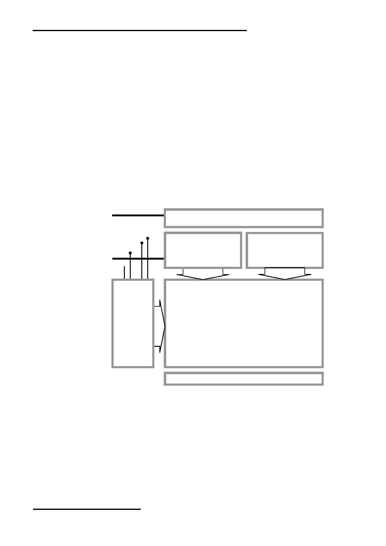
1.3 Block Diagram
VDD,VSS
VEE
Power Circuit
LP
SEG
SEG
CP
Driver
Driver
/DISPOFF
D0~D3
FLM
COM1
320 x 240 pixels
:
LCD Panel
COM240
BLA, BLK
Backlight Circuit
URL: www.topwaydisplay.com
Document Name: LM32019TFW-Manual-Rev0.5
Page: 3 of 9
TOPWAY
LCD Module User Manual
LM32019TFW
1.4 FFC Terminal Functions
Pin
Pin
No.
Name
I/O
Descriptions
1
FLM
Input
First Line Marker
2
LP
Input
Line Pulse signal,
for latching the segment buffer to the segment driver
3
CP
Input
Clock Pulse signal,
for shifting the data (D0~D3) into the segment buffer
4
NC
Input
No connection (leave open)
5
/DISPOFF
Input
Display ON/OFF control signal,
/DISPOFF = 0, display off
/DISPOFF = 1, display on
6
D0
Input
Display Data
7
D1
Input
Display Data
8
D2
Input
Display Data
9
D3
Input
Display Data
10
VDD
Power Positive Power Supply
11
VSS
Power 0V Power Supply, GND
12
VEE
Input
LCD Driving Supply
1.5 Backlight Terminal Functions
Pin
Pin
Color
Name
I/O
Descriptions
Red
BLA
Power Positive Power Supply for LED backlight
White
BLK
Power Negative Power Supply for LED backlight
URL: www.topwaydisplay.com
Document Name: LM32019TFW-Manual-Rev0.5
Page: 4 of 9
TOPWAY
LCD Module User Manual
LM32019TFW
2. Absolute Maximum Ratings
Items
Symbol
Min.
Max.
Unit
Condition
Logic Supply
V DD
-0.3
+6.0
V
V SS = 0V
LCD Driving Supply
V EE
-0.3
+30.0
V
V SS = 0V
Input Voltage
V IN
V SS -0.3
V DD +0.3
V
V SS = 0V
Operating Temperature
T OP
-20
70
C
No Condensation
Storage Temperature
T ST
-30
80
C
No Condensation
Cautions:
Any Stresses exceeding the Absolute Maximum Ratings may cause substantial damage to the device. Functional operation of this
device at other conditions beyond those listed in the specification is not implied and prolonged exposure to extreme conditions may
affect device reliability.
3. Electrical Characteristics
3.1 DC Characteristics
V SS =0V, V DD =5.0V, T OP =25 C
Items
Symbol
MIN.
TYP.
MAX.
Unit Applicable Pin
Logic Supply
V DD
3.0
5.0
5.3
V
VDD
LCD Driving Supply
V EE
-
22.6
-
V
VEE (*1)
Frame Freq.
f FRAME
60
66
80
Hz
D0~D3, CP, LP,
Input High Voltage
V IN
0.8xVDD
-
VDD
V
FLM, M, /DISPOFF
D0~D3, CP, LP,
Input Low Voltage
V IN
0
-
0.2x VDD
V
FLM, M, /DISPOFF
Operating Current
I DD
-
0.1
0.5
mA VDD
LCD Driving current
I EE
-
2.0
10.5
mA VEE
Note:
*1. Frame freq. at 66Hz
3.2 LED Backlight Circuit Characteristics
BLK=0V, If BLA =153mA, T OP =25 C
Items
Symbol
MIN.
TYP.
MAX.
Unit
Applicable Pin
Forward Voltage
Vf BLA
-
5.0
-
V
BLA
Forward Current
If BLA
-
153
200
mA
BLA
Cautions:
Exceeding the recommended driving current could cause substantial damage to the backlight and shorten its lifetime.
BLA
BLK
No. of LED = 9pcs
URL: www.topwaydisplay.com
Document Name: LM32019TFW-Manual-Rev0.5
Page: 5 of 9

TOPWAY
LCD Module User Manual
LM32019TFW
3.3 AC Characteristics
V SS =0V, T OP =25 C
V DD =5.0V
V DD =3.3V
Item
Symbol
MIN.
MAX.
MIN.
MAX.
Unit
Shift clock period (*1)
twck
90
-
160
-
ns
Shift clock “H” pulse width
twckh
30
-
64
-
ns
Shift clock “L” pulse width
twckl
30
-
64
-
ns
SEG Data set-up time
tds
13
-
38
-
ns
SEG Data hold time
tdh
13
-
50
-
ns
Latch pulse “H” pulse width
twlph
30
-
64
-
ns
Shift clock rise to latch pulse rise time
tld
9
-
9
-
ns
Shift clock fall to latch pulse fall time
tsl
32
-
64
-
ns
Latch pulse rise to shift clock rise time
tls
32
-
64
-
ns
Latch pulse fall to shift clock fall time
tlh
32
-
64
-
ns
Rise time
tr
-
40
-
40
ns
Fall time
tf
-
40
-
40
ns
/DISPOFF removal time
tsd
125
-
125
-
ns
/DISPOFF “L” pulse width
twdl
1500
-
1500
-
ns
COM Data setup time
tsu
38
-
38
-
ns
COM Data hold time
th
63
-
63
-
ns
Note: *1. tr, tf < 9ns
Interface Timing Digram
URL: www.topwaydisplay.com
Document Name: LM32019TFW-Manual-Rev0.5
Page: 6 of 9
TOPWAY
LCD Module User Manual
LM32019TFW
4. Function Specifications
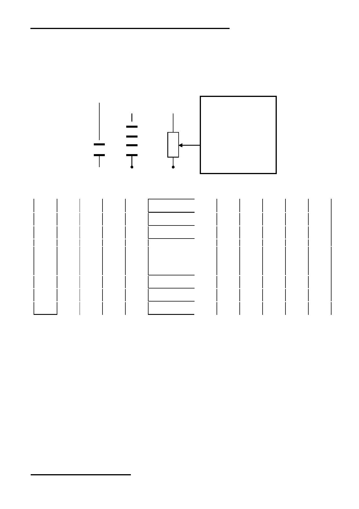
4.1 Adjusting the Display Contrast
Adjusting the LCD Driving Supply on the VEE will result the change of LCD display contrast.
The following is a simplest circuit to provide a variable voltage on VEE.
LCD module
VDD
VR
VEE
VSS
4.2 Display Pixel Map
1,1
2,1
3,1
4,1
5,1
316,1
317,1
318,1
319,1
320,1
(D3)
(D2)
(D1)
(D0)
(D3)
- - -
- - -
(D0)
(D3)
(D2)
(D1)
(D0)
1,2
2,2
3,2
4,2
5,2
316,2
317,2
318,2
319,2
320,2
(D3)
(D2)
(D1)
(D0)
(D3)
- - -
- - -
(D0)
(D3)
(D2)
(D1)
(D0)
1,3
2,3
3,3
4,3
5,3
316,3
317,3
318,3
319,3
320,3
(D3)
(D2)
(D1)
(D0)
(D3)
- - -
- - -
(D0)
(D3)
(D2)
(D1)
(D0)
:
:
:
:
:
:
:
:
:
:
:
:
:
:
:
:
:
:
:
:
:
:
:
:
:
:
:
:
:
:
:
:
:
:
:
:
1,238
2,238
3,238
4,238
5,238
316,238 317,238 318,238 319,238 320,238
(D3)
(D2)
(D1)
(D0)
(D3)
- - -
- - -
(D0)
(D3)
(D2)
(D1)
(D0)
1,239
2,239
3,239
4,239
5,239
316,239 317,239 318,239 319,239 320,239
(D3)
(D2)
(D1)
(D0)
(D3)
- - -
- - -
(D0)
(D3)
(D2)
(D1)
(D0)
1,240
2,240
3,240
4,240
5,240
316,240 317,240 318,240 319,240 320,240
(D3)
(D2)
(D1)
(D0)
(D3)
- - -
- - -
(D0)
(D3)
(D2)
(D1)
(D0)
Pixel mapping (Top View)
Based on the top view of the LCD module,
the 1, 1 (x, y) pixel is the upper-left pixel;
the 320, 240 (x, y) pixel is the lower-right pixel.
URL: www.topwaydisplay.com
Document Name: LM32019TFW-Manual-Rev0.5
Page: 7 of 9

TOPWAY
LCD Module User Manual
LM32019TFW
4.3 Signal Sequence
In the upper section (expended view), shows the data sequence of lines.
In the lower section (compressed view), shows the signal sequence of FLM, LP and M in frames.
URL: www.topwaydisplay.com
Document Name: LM32019TFW-Manual-Rev0.5
Page: 8 of 9

TOPWAY
LCD Module User Manual
LM32019TFW
5. Design and Handling Precaution
Please refer to "LCD-Module-Design-Handling-Precaution.pdf".
6. Reliability Test
Test Items
Testing Condition
Note
High Temperature Storage
Duration = 96 hours,
Non-operating
Temperature = +80°C±5°C
Low Temperature Storage
Duration = 96 hours,
Non-operating
Temperature = -30°C±5°C
High Temperature Operation
Duration = 96 hours,
Operating
Temperature = +70°C±5°C
Low Temperature Operation
Duration = 96 hours,
Operating
Temperature = -20°C±5°C
Thermal Shock
10 cycle of
Non-operating
-30°C (30min) Room Temp. (<5min)
+80°C (30min) Room Temp. (<5min)
Vibration
50Hz, 2~3mm, Duration = 2 hours
Non-operating
Temperature = Room Temp.
Drop Test
Drop form 60cm above ground
Non-operating
(whole package with same weight)
4-faces, 6-edge, 2-corner
Note:
*1. After the test, keep the test sample at room temperature for 2hours (no condensation).
There should no failure of display quality and appearance.
There should not have any abnormality of functions.
URL: www.topwaydisplay.com
Document Name: LM32019TFW-Manual-Rev0.5
Page: 9 of 9