LM6066RDW
LCD Module User Manual
Prepared by:
Checked by:
Approved by:
Date:
Date:
Date:
Rev. Descriptions
Release Date
0.1
New release
2010-12-31
URL: www.topwaydisplay.com
Document Name: LM6066RDW-Manual-Rev0.1
Page: 1 of 12

TOPWAY
LCD Module User Manual
LM6066RDW
Table of Content
1. Basic Specifications .............................................................................................................. 3
1.1
Display Specifications .......................................................................................................... 3
1.2
Mechanical Specifications .................................................................................................... 3
1.3
Block Diagram ...................................................................................................................... 3
1.4
Terminal Functions ............................................................................................................... 4
2. Absolute Maximum Ratings .................................................................................................. 5
3. Electrical Characteristics ...................................................................................................... 5
3.1
DC Characteristics ............................................................................................................... 5
3.2
LED Backlight Circuit Characteristics ................................................................................... 5
3.3
AC Characteristics ................................................................................................................ 6
3.4
Reset Timing ........................................................................................................................ 6
4. Function Specifications ......................................................................................................... 7
4.1
Adjusting the Display Contrast .............................................................................................. 7
4.2
Resetting the LCD module ................................................................................................... 7
4.3
Interfacing Setting ................................................................................................................ 7
4.4
Display Pixel Map ................................................................................................................. 7
4.5
Control Data and Command ................................................................................................. 8
4.6
Command Summary ............................................................................................................ 8
5. Design and Handling Precaution ........................................................................................ 12
URL: www.topwaydisplay.com
Document Name: LM6066RDW-Manual-Rev0.1
Page: 2 of 12
TOPWAY
LCD Module User Manual
LM6066RDW
1. Basic Specifications
1.1 Display Specifications
1) LCD Display Mode
: STN-Gray, Positive, Transflective
2) Display Color
: Display Data = “1” : Dark Blue (*1)
: Display Data = “0” : Light Gray (*2)
3) Viewing Angle
: 6H
4) Driving Method
: 1/64 duty, 1/8.2 bias
5) Backlight
: White LED backlight
Note:
*1. Color tone may slightly change by Temperature and Driving Condition.
*2. The Color is defined as the inactive / background color
1.2 Mechanical Specifications
1) Outline Dimension
: 180.0 x 62.0 x 12.3 MAX.
see attached Outline Drawing for details
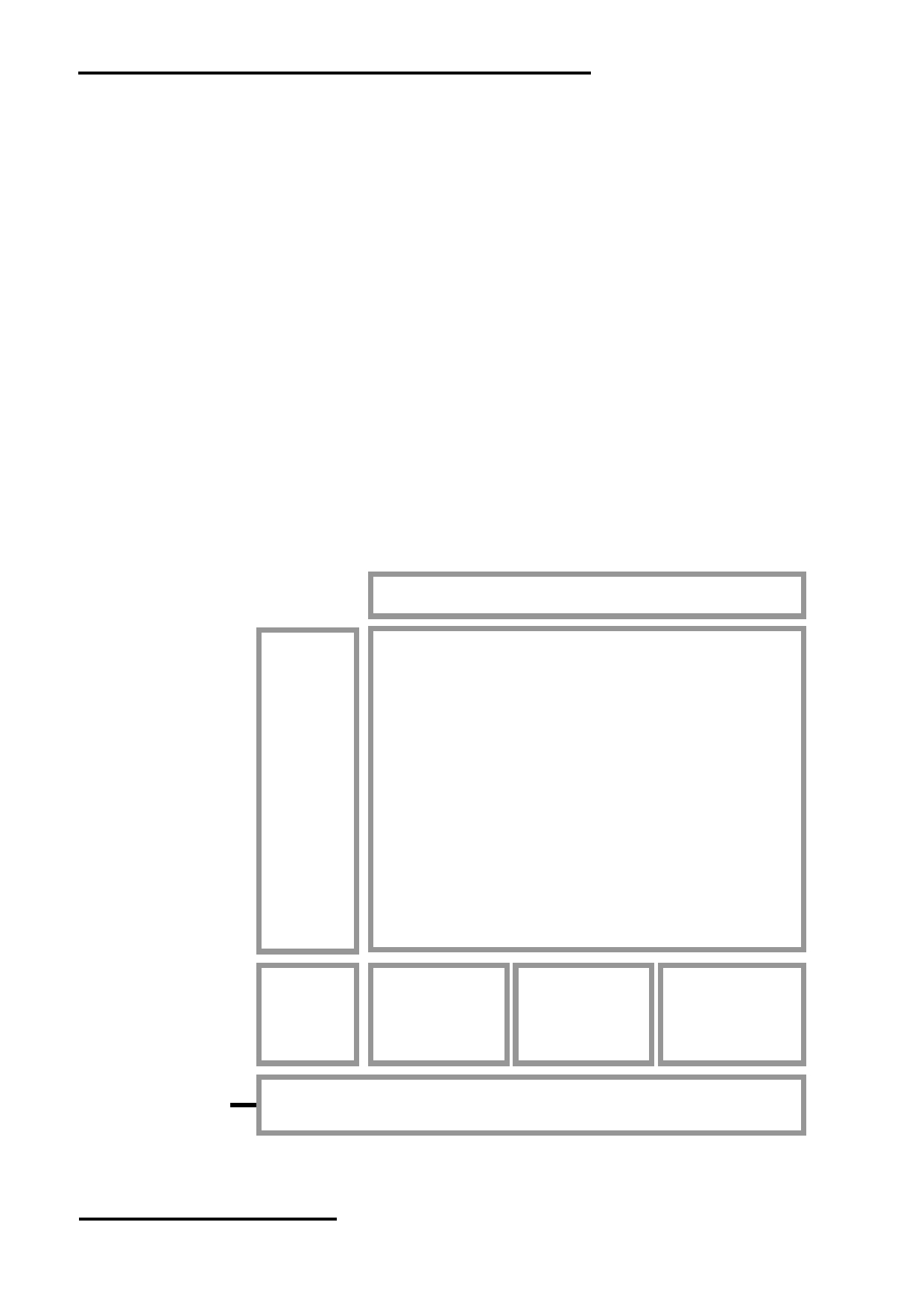
1.3 Block Diagram
BLA
BLK
Backlight Circuit
240 x 64 pixels
LCD Panel
VDD
VSS
Booster &
VOUT
Power Circuit
SEGMENT
SEGMENT
SEGMENT
V0
Driver
Driver
Driver
/WR,/RD,RS, /CS,/RST
DB0~DB7
RA8806
BUSY
or equivalent
URL: www.topwaydisplay.com
Document Name: LM6066RDW-Manual-Rev0.1
Page: 3 of 12

TOPWAY
LCD Module User Manual
LM6066RDW
1.4 Terminal Functions
Pin No.
Pin
K1
Name
I/O
Descriptions
1
VOUT
Power
Power Booster Output for V0
2
V0
Input
LCD Contrast Reference Input
3
VSS
Power
0V Power Supply, GND
4
VDD
Power
Positive Power Supply
5
BUSY
Output
Indicate the RA8806 in busy state or not,could been used for
MPU to get busy state by connecting it to IO port
6
NC
NC
No connection,leave open
7
/CS
Input
Chip Select Signal
/CS=LOW: Data IO is enabled
Register Select
8
RS
Input
RS=HIGH: write address of register and read status word
RS=LOW: write & read data of register and DDRAM
9
/WR
Input
Write enable input, active LOW
10
/RD
Input
Read enable input, active LOW
11
DB0
:
:
I/O
8-bit bi-directional data bus
18
DB7
Reset Signal:
19
/RST
Input
/RST = L, Reset the LCD Module
/RST = H, Normal Running
20
NC
NC
No connection,leave open
21
BLA
Power
Positive Power Supply for LED backlight
22
BLK
Power
Negative Power Supply for LED backlight
23
BLA
Power
Positive Power Supply for LED backlight
24
BLK
Power
Negative Power Supply for LED backlight
25
BLA
Power
Positive Power Supply for LED backlight
26
BLK
Power
Negative Power Supply for LED backlight
note:
*1. The LCM Fixed to 80 mode by default ,could been changed to 68 mode by changing jumpers
URL: www.topwaydisplay.com
Document Name: LM6066RDW-Manual-Rev0.1
Page: 4 of 12
TOPWAY
LCD Module User Manual
LM6066RDW
2. Absolute Maximum Ratings
Items
Symbol
Min.
Max.
Unit
Condition
Supply Voltage
V DD
0
+3.3
V
V SS = 0V
Input Voltage
V IN
V SS -0.3
V DD +0.3
V
V SS = 0V
Operating Temperature
T OP
-20
+70
C
No Condensation
Storage Temperature
T ST
-30
+80
C
No Condensation
Cautions:
Any Stresses exceeding the Absolute Maximum Ratings may cause substantial damage to the device. Functional operation of this
device at other conditions beyond those listed in the specification is not implied and prolonged exposure to extreme conditions may
affect device reliability.
3. Electrical Characteristics
3.1 DC Characteristics
V SS =0V, V DD =3.3V, T OP =25 C
Items
Symbol
MIN.
TYP.
MAX.
Unit Applicable Pin
Operating Voltage
V DD
3.0
3.3
3.6
V
VDD
DB0~DB7, /WR, /RD, /CS,
Input High Voltage
V IN
0.8VDD
-
VDD
V
RS, /RST
DB0~DB7, /WR, /RD, /CS,
Input Low Voltage
V IN
VSS
-
0.1VDD
V
RS, /RST
LCD Contrast
V0
Reference Voltage
V 0
-
11.7
-
V
Operating Current
I DD
-
9.0
25
mA VDD
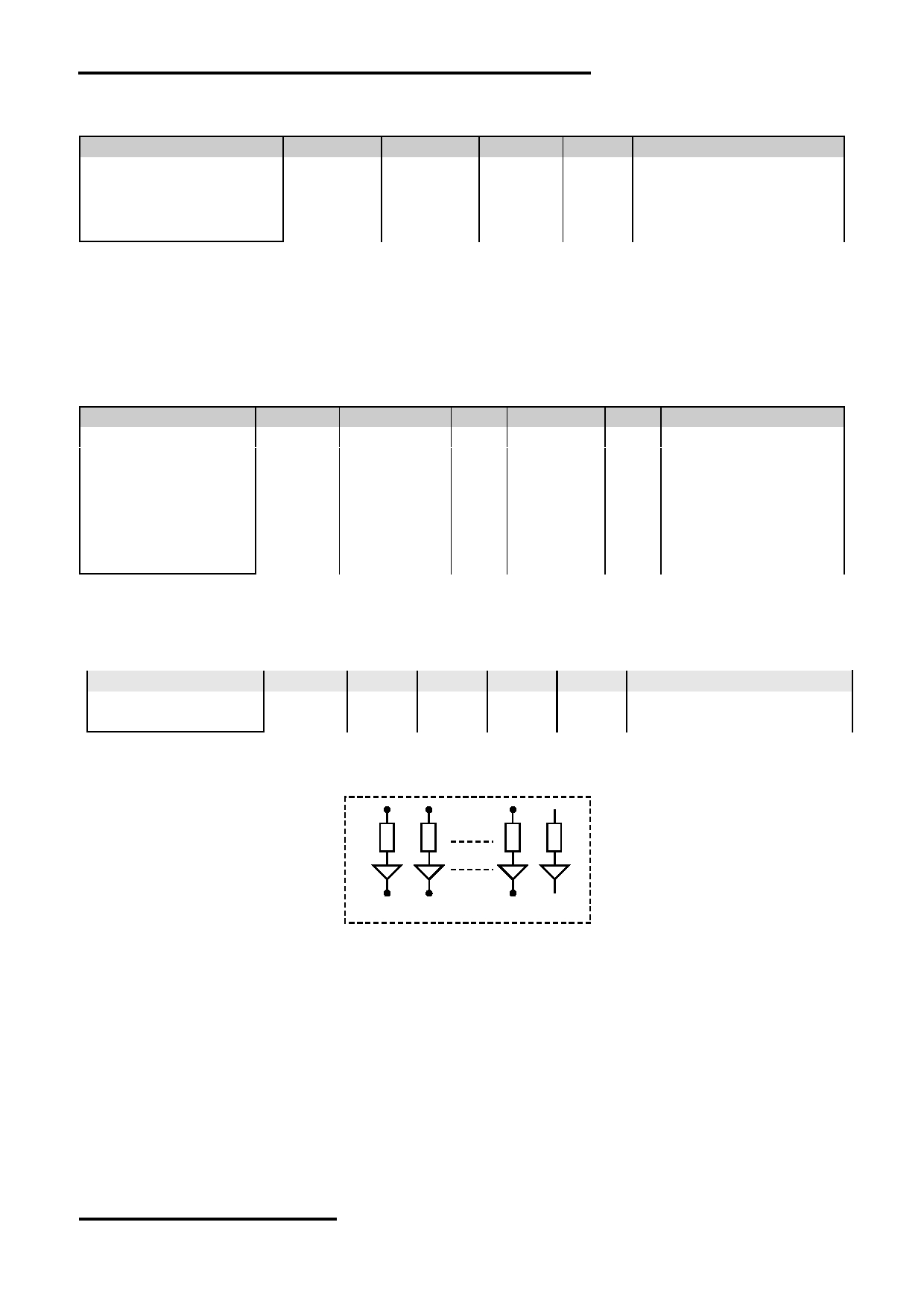
3.2 LED Backlight Circuit Characteristics
BLK=0V, If BLA =102mA, T OP =25 C
Items
Symbol
MIN.
TYP.
MAX.
Unit
Applicable Pin
Forward Voltage
Vf BLA
-
3.3
-
V
BLA
Forward Current
If BLA
-
102
120
mA
BLA
Cautions:
Exceeding the recommended driving current could cause substantial damage to the backlight and shorten its lifetime.
BLA
BLK
No. of LED = 6 pcs
URL: www.topwaydisplay.com
Document Name: LM6066RDW-Manual-Rev0.1
Page: 5 of 12
TOPWAY
LCD Module User Manual
LM6066RDW
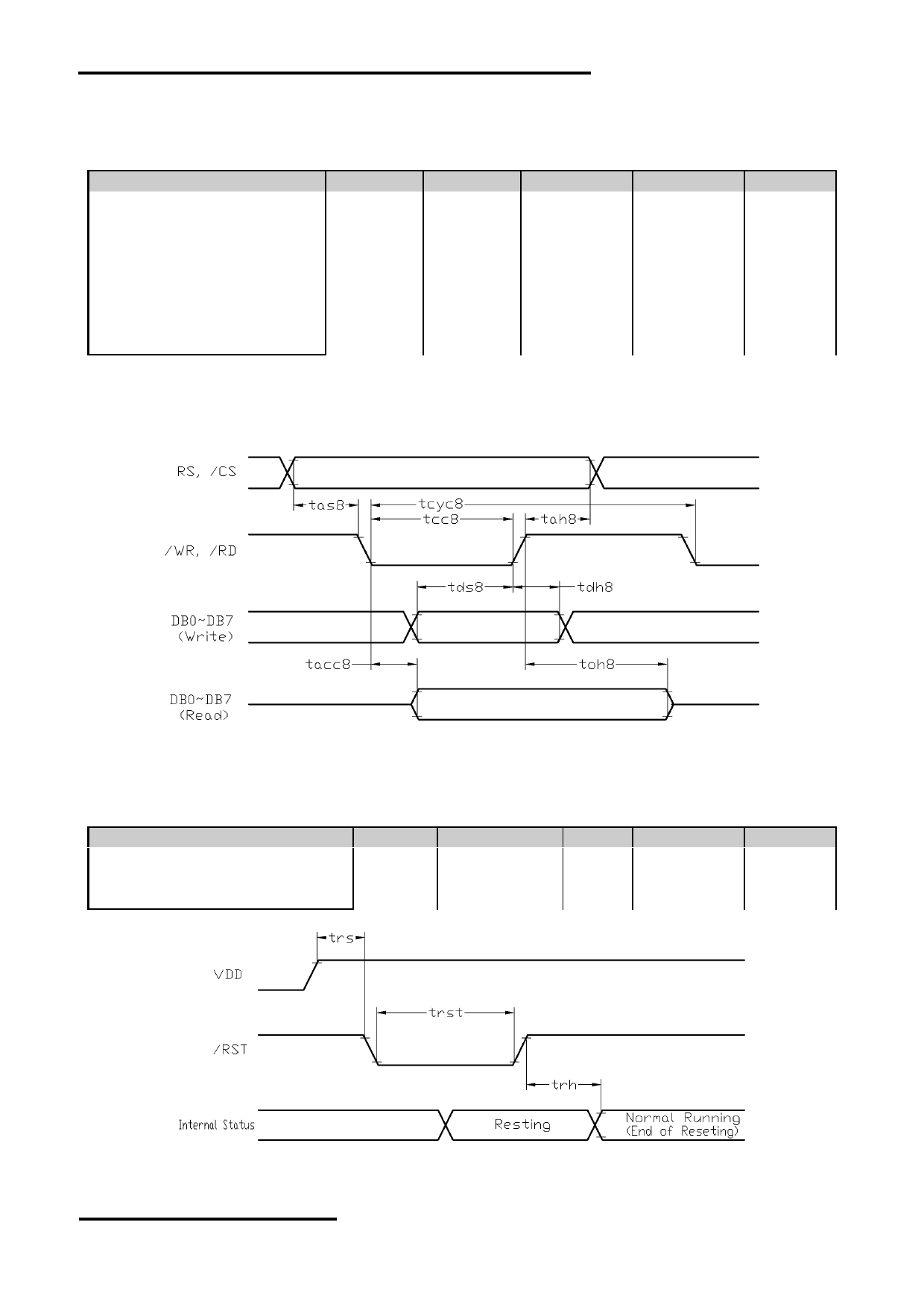
3.3 AC Characteristics
3.3.1 8080 Mode
V SS =0V, V DD =3.3V, T OP =25 C
Item
Symbol
MIN.
TYP.
MAX.
Unit
System Cycle Time (*2)
tcyc8
320
-
-
ns
Strobe Pulse Width
tcc8
63
-
-
ns
Address Setup Time
tas8
10
-
-
ns
Address Hold Time
tah8
25
-
-
ns
Data Setup Time
tds8
38
ns
Data Hold Time
tdh8
25
-
-
ns
Data Access Time
tacc8
-
-
25
ns
Output disable Time
toh8
-
-
13
ns
Note: *1. Input signal rise/fall time should be less than 20ns
*2. System clock=6MHz
*3. Bus timing is for one byte transaction only.
For details, please refer to RA8806 datasheet.
Bus Timing Diagram
3.4 Reset Timing
V SS =0V, V DD =3.3V, T OP =25 C
Item
Symbol
MIN.
TYP.
MAX.
Unit
Reset setup time
trs
1.3
-
-
ms
Reset hold time
trh
1.3
-
-
ms
Reset active time (*1)
trst
0.2
-
-
us
Note: *1. System clock=6MHz
Reset Timing Diagram
URL: www.topwaydisplay.com
Document Name: LM6066RDW-Manual-Rev0.1
Page: 6 of 12
TOPWAY
LCD Module User Manual
LM6066RDW
4. Function Specifications
4.1 Adjusting the Display Contrast
VDD
A Variable-Resistor must be connected to the
LCD module for providing a reference to V0.
Adjusting the VR will result the change of
LCD display contrast.
VR
V0
The recommended value of VR is 25k to 50k
VOUT
VSS
4.2 Resetting the LCD module
The LCD module should be initialized by hardware reset, using /RST terminal.
While turning on the VDD and VSS power supply, maintain /RST terminal at LOW level. After the
power supply stabilized, release the reset terminal (/RST=HIGH)
4.3 Interfacing Setting
Jumpers could been used to change bus interfacing family
Jumper
JP6
JP7
JP8
JP9
Function Discription
open
close
close
open
8080 mode 8 bit selected <default>
open
open
close
close
6800 mode 8 bit selected
close
open
open
close
6800 mode 4 bit selected
4.4 Display Pixel Map
1,1
2,1
3,1
4,1
5,1
236,1
237,1
238,1
239,1
240,1
(D7)
(D6)
(D5)
(D4)
(D3)
- - -
- - -
(D4)
(D3)
(D2)
(D1)
(D0)
1,2
2,2
3,2
4,2
5,2
236,2
237,2
238,2
239,2
240,2
(D7)
(D6)
(D5)
(D4)
(D3)
- - -
- - -
(D4)
(D3)
(D2)
(D1)
(D0)
1,3
2,3
3,3
4,3
5,3
236,3
237,3
238,3
239,3
240,3
(D7)
(D6)
(D5)
(D4)
(D3)
- - -
- - -
(D4)
(D3)
(D2)
(D1)
(D0)
:
:
:
:
:
:
:
:
:
:
:
:
:
:
:
:
:
:
:
:
:
:
:
:
:
:
:
:
:
:
:
:
:
:
:
:
1, 62
2, 62
3, 62
4, 62
5, 62
236,262 237, 62 238,262 239, 62
240,62
(D7)
(D6)
(D5)
(D4)
(D3)
- - -
- - -
(D4)
(D3)
(D2)
(D1)
(D0)
1, 63
2, 63
3, 63
4, 63
5, 63
236, 63 237, 63 238, 63 239,263 240,63
(D7)
(D6)
(D5)
(D4)
(D3)
- - -
- - -
(D4)
(D3)
(D2)
(D1)
(D0)
1, 64
2, 64
3, 64
4, 64
5, 64
236, 64 237, 64 238,264 239, 64
240,64
(D7)
(D6)
(D5)
(D4)
(D3)
- - -
- - -
(D4)
(D3)
(D2)
(D1)
(D0)
Pixel mapping (Top View)
Note:
*1.
Based on the top view of the LCD module,
the 1, 1 (x, y) pixel is the upper-left pixel;
the 240, 64 (x, y) pixel is the lower-right pixel.
*2.
For the details of memory mapping please refer to RA8806 datasheet.
URL: www.topwaydisplay.com
Document Name: LM6066RDW-Manual-Rev0.1
Page: 7 of 12
TOPWAY
LCD Module User Manual
LM6066RDW
4.5 Control Data and Command
The LCD module setting is controlled by the internal Register Values.
The Register Address should be addressed when RS=1 and Register Value should be issued
when RS=0.
A full command sequence should be as follow.
Steps
/RD
/WR
RS
Data (DB0~ DB7)
1 st
1
0
1
Register Address
2 nd
1
0
0
Register Value
4.6 Command Summary
Note:
For details please refer to RA8806 datasheet.
Reg.
Reg.
Add
Name R/W
Descriptions
MBUSY: Memory Write Busy Flag
1=Busy when write font or clear RAM; 0=not busy
SBUSY: Scan Busy Flag
1=Busy when driver scan logic is not idle; 0=not busy
SLEEP: Sleep state
1= In Sleep mode; 0=In Normal mode
WAKE_STS: Wakeup Status Bit Same as REG[0FH] Bit2
KS_STS: Key Status Bit
Same as REG[0FH] Bit1
--
STATUS
R
TP_STS: Tp Status Bit
Same as REG[0FH] Bit0
00h
WLCR R/W
PWR : Power Mode
1=In Sleep Mode; 0=In Normal Mode
LINER: linear Decode Mode
1=User-defined ROM mapping rule; 0=GIG5/GB ROM mapping
rule
SR : Software Reset
1=reset all register (except DDRAM); 0=normal operation
CG : Display mode selection
1=Character Mode; 0=Graphic Mode
DP : Display on off control
1=normal display; 0=display off
BK : Full screen blinking control
1=blinking (blink time is set by REG 80H); 0=normal;
DV : Full screen inverse control
1=Inverse Full Screen; 0=Normal
01h
MISC
R/W
NO_FLICKER : Eliminating Flicker
1=enable, scan will auto-pending when busy; 0=disable
CKN : Clock Output in pin CLK_OUT
1=The pin indicates SLEEP state of STATUS REG;
0=The pin output internal system clock
BUSY_LEV : Busy Polarity(for “BUSY” pin)
1=Set Active High; 0=Set Active Low
INT_LEV: Interrupt Polarity (for “INT” pin)
1=Set Active High; 0=Set Active Low
XCK_SEL[1:0] : Driver Clock Selection
00=CLK/8; 01=CLK/4(Default); 10=CLK/2; 11=CLK
The CLK means system clock
SDIR:SEG Scan Direction
1=SEG order is 319~0; 0=SEG order is 0~319
CDIR: COM Scan Direction
1=COM order is 239~0; 0=COM order is 0~239
03h
ADSR R/W
SCR_PEND : scroll Function Pending
1=Scroll function pending; 0=Scroll function keep active
BIT_INV : Set driver data output BIT Order
1=inverse order (BIT7 to BIT0, BIT6 to BIT1, and so on;
0=Normal order
SCR_DIR : Scroll Direction
When SCR_HV=1, 1= Bottom -> Top; 0= Top -> Bottom
When SCR_HV=0, 1=Right -> Left; 0=Left -> Right
SCR_HV : Scroll Horizontal/Vertical Selection
1= Common Scrolling(Vertical); 0= Segment Scrolling(Horizontal)
SCR_EN : Scroll Enable
1=Scroll function enable; 0=Scroll function disable
URL: www.topwaydisplay.com
Document Name: LM6066RDW-Manual-Rev0.1
Page: 8 of 12
TOPWAY
LCD Module User Manual
LM6066RDW
Register Table Summary (cont’)
Reg.
Reg.
Add
Name R/W
Descriptions
0FH
INTR
R/W
WAKI_EN : Wakeup Interrupt Mask
1=enable ; 0=disable
KEYI_EN : Key-Scan Interrupt Mask
1=enable ; 0=disable
TPI_EN : Touch Panel Interrupt Mask
1=Generate interrupt output if TP was detected; 0=disable
TP_ACT : Touch Panel Event (only read)
1=TP is touched;0=TP is not touched
WAK_STS : Wakeup Interrupt Status bit
1=Indicate wake-up event happen from Sleep mode
0=Indicate no wake-up happen
User must write 0 to clear the status bit
KEY_STS : Key-Scan Interrupt Status bit
1=Key-Scan Detect Key input; 0=Key-Scan don’t Delete key input
User must write 0 to clear the status bit
TP_STS : Touch Panel Detect Status bit
1= TP touched; 0=TP untouched
User must write 0 to clear the status bit
10h
WCCR R/W
CUR_INC : Auto-increase Cursor Position in reading/writing
DDRAM operation
1=disable; 0=enable
FILL_OFS: Full-size and Half-size Character Alignment
1=Full-size alignment in Full-size and Half-size mixed mode;
0=disable
BIT_REV : Reversed Data Write mode
1= inversely; 0= directly
BOLD : Set Bold font (char mode only)
1=bold; 0=normal
T90DEG : Font Rotate mode (Font rotated 90 degree)
1=enable; 0=normal
CUR_EN : Cursor display control
1=on; 0=off
CUR_BLK : Cursor blink control
1=blinking; 0=normal (Blink time is determined by REG 80H)
11h
CHWI
R/W
CURH[3:0] : Cursor Height (Vertical direction, horizontal is fix)
0000b : Cursor height 1pixel
0001b : Cursor height 2 pixels
……
1111b : Cursor height 16 pixels
ROWH[3:0] : Char Line Gap
0000b : Char LineGap 1pixel
0001b : Char LineGap 2 pixels
……
1111b : Char LineGap 16 pixels
12h
MAMR R/W
CUR_HV : Cursor Auto Shifting Direction(only Graphic Mode)
1= Vertical then Horizontal; 0= Horizontal then Vertical
DISPMD[2:0] : Display Layer and Display Mode Selection
001=page1 only(default); 010=page2 only;
011=combine two layer; 000=gray scale mode
110=extended mode1, 111=extended mode2
L_MIX[1:0] : two layer mode setting
00=OR; 01=XOR; 10=NOR; 11=AND
MW[1:0] : Layer Read/Write Selection
00=CGRAM(512Byte); 01=page1; 10=page2;
11=page1 & page2 at the same time
20h
AWRR R/W
AWR[5:0]: Active Window Right Position ->Segment-Right
Default Value:27h
21h
DWRR R/W
DWW[5:0] : Display Window Width Position -> Segment-Width
Segment-Width = (Segment Number / 8) – 1
Default Value:27h
30h
AWBR R/W
AWT[7:0] : Active Window Bottom Position->Common-Bottom
Default Value: efh
31h
DWHR R/W
DWH[7:0] : Display Window Bottom Position->Common-Height
Common-Height = LCD Common Number – 1
Default Value: efh
URL: www.topwaydisplay.com
Document Name: LM6066RDW-Manual-Rev0.1
Page: 9 of 12
TOPWAY
LCD Module User Manual
LM6066RDW
Register Table Summary (cont’)
Reg.
Reg.
Add
Name R/W
Descriptions
40h
AWLR R/W
AWL[5:0] : Active Window Left Position-> Segment-Left
Default Value:00h
50h
AWTR R/W
AWT[7:0] : Active Window Top Position -> Common- Top
Default Value:00h
60h
CURX R/W
CURX[5:0] : Cursor Position of Segment /CGRAM address[4:0]
61h
BGSG R/W
BGSG[5:0] : Segment Start Position of Scrolling Mode
62h
EDSG R/W
EDSG[5:0] : Segment End Position of Scrolling Mode
70h
CURY R/W
RC7~RC0 : Cursor Position of Common /CGRAM address[8:5]
71h
BGCM R/W
BGCM[7:0] : Common Start Position of Scrolling Mode
72h
EDCM R/W
EDCN[7:0] : Common Ending Position of Scrolling Mode
80h
BTMR R/W
BLKT[7:0] : Cursor Blink Time and Scroll Time
Blinking Time = Bit[7:0] x (Frame width)
Frame width = 1 / Frame Rate
90h
ITCR
R/W
ITC[7:0] : Idle Time Setting, In count of system clock
FR_time = COM_NO x ( SEG_NO / 4 + ITC ) / XCK
FR_time = 1 / Frame Rate
A0h
KSCR1 R/W
KSCR1[7] : Key Scan Enable
1=enable, 0=disable
KSCR1[6] : Key Scan Enable
1 : 4x8 Matrix(KOUT[3:0] is used, KOUT[7:4] please keep floating)
0 : 8x8 Matrix(KOUT[7:0] is used)
KSCR1[5:4] : Key Scan Data Sampling Times
00: 4, 01: 8, 10: 16, 11:32
KSCR1[3] : Long Time Key Function
1=enable, 00=disable
KSCR1[2:0] : Key Scan Freq
A1h
KSCR2 R/W
KSCR2[7] : Key Scan Wakeup Function
1=enable, 0=disable
KSCR2[3:2] : Long Key Timing Adjustment
KSCR2[1:0] : Number of Key Hit
A2h
KSDR0
R
KSDR0[7:0] : Key Strobe Data
A3h
KSDR1
R
KSDR1[7:0] : Key Strobe Data
A4h
KSDR2
R
KSDR2[7:0] : Key Strobe Data
URL: www.topwaydisplay.com
Document Name: LM6066RDW-Manual-Rev0.1
Page: 10 of 12
TOPWAY
LCD Module User Manual
LM6066RDW
Register Table Summary (cont’)
B0h
MWCR
W
MWD[7:0] : The Data is written to memory under the cursor
position
B1h
MRCR
R
MRD[7:0] : The Data is Read from memory under the cursor
position
C0h
TPCR1 R/W
TPCR1[7] : Touch Panel Enable
1=enable, 0=disable
TPCR1[6:4] : Touch Panel Sample Time adjustment
TPCR1[3] : Touch Panel Wake-Up
1=enable, 0=disable
TPCR1[2:0] : Touch Panel ADC Convert Speed
C1h
TPXR
R
TPXR[7:0] : Touch Panel X Data Bit[9:2]
C2h
TPYR
R
TPYR[7:0] : Touch Panel Y Data Bit[9:2]
C3h
TPZR
R
TPZR[3:2] : Touch Panel Y Data Bit[1:0]
TPZR[1:0] : Touch Panel X Data Bit[1:0]
C4h
TPCR2 R/W
TPCR2[7] : TP Manual Mode
1=manual mode, 0=auto mode
TPCR2[1:0] : TP manual mode Options
E0h
PNTR R/W
PND[7:0] : Data Written to DDRAM when REGF0H Bit3=1
F0h
FNCR R/W
ISO8859_EN : ISO8859 Mode
1=disable; 0=enable
MCLR : Memory Clear function
1=enable fill data of REG E0H to DDRAM under Active Window
area; 0=no action;
ASC : Font ROM range select
1=decode as ASCII; 0=auto treat as ASCII or GB
ASC_SEL[1:0] : ASCII Block Selection
00=map to ASCII block 1; 01=map to ASCII block 2;
10=map to ASCII block 3; 11=map to ASCII block 4
F1h
FVHT
R/W
FH1~FV0 : Font Horizontal Size
00=1x; 01=2x; 10=3x; 11=4x
FV1~FV0 : Font Vertical Size
00=1x; 01=2x; 10=3x; 11=4x
Note:
*1. It is suggested to check the BUSY before sending the Control Data.
*2. For the details, please refer to RA8806 Data sheet.
URL: www.topwaydisplay.com
Document Name: LM6066RDW-Manual-Rev0.1
Page: 11 of 12

TOPWAY
LCD Module User Manual
LM6066RDW
5. Design and Handling Precaution
Please refer to "LCD-Module-Design-Handling-Precaution.pdf".
URL: www.topwaydisplay.com
Document Name: LM6066RDW-Manual-Rev0.1
Page: 12 of 12