TM033XDHG01-00
MODEL NO. :
TM033XDHG01-00
ISSUED DATE:
2016-11-21
VERSION
:
Ver 1.0
■Preli minary Specification
□Final Product Specification
Customer :
Approved by
Notes
SHANGHAI TIANMA Confirmed :
Prepared by
Checked by
Approved by
This technical specification is subjected to change without notice
The information contained herein is the exclusive property of TIANMA MICRO-ELECTRONICS
Corporation and shall not be distributed, reproduced, or disclosed in whole or in part without prior written
permission of TIANMA MICRO-ELECTRONICS Corporation.
Page 1 of 19

TM033XDHG01-00
Table of Contents
Table of Contents............................................................................................................................ 2
Record of Revision ......................................................................................................................... 3
1
General Specifications ............................................................................................................. 4
2
Input/Output Terminals ............................................................................................................. 5
3
Absolute Maximum Ratings ..................................................................................................... 6
4
Electrical Characteristics .......................................................................................................... 7
5
Timing Chart ............................................................................................................................ 9
6
Optical Characteristics ............................................................................................................13
7
Environmental / Reliability Tests ..............................................................................................16
8
Mechanical Drawing ...............................................................................................................17
9
Packing Drawing .....................................................................................................................18
10 Precautions for Use of LCD Modules ......................................................................................19
The information contained herein is the exclusive property of TIANMA MICRO-ELECTRONICS
Corporation and shall not be distributed, reproduced, or disclosed in whole or in part without prior written
permission of TIANMA MICRO-ELECTRONICS Corporation.
Page 2 of 19
TM033XDHG01-00
Record of Revision
Rev
Issued Date
Description
Editor
1.0
2016-11-21 Preliminary spec release
Jin Zhao
The information contained herein is the exclusive property of TIANMA MICRO-ELECTRONICS
Corporation and shall not be distributed, reproduced, or disclosed in whole or in part without prior written
permission of TIANMA MICRO-ELECTRONICS Corporation.
Page 3 of 19
TM033XDHG01-00
1 General Specifications
Feature
Spec
Size
3.34inch
Resolution
320(RGB) X 320
Interface
MIPI (Command Mode)
Color Depth
16M dithering
Technology Type
a-si TFT
Display Spec.
Pixel pitch(mm)
0.1875 x 0.1875
Pixel Configuration
R.G.B. Vertical Stripe
Display Mode
TM with Normally White
Surface Treatment
HC
Viewing Direction
12 o’clock
Gray Scale Inversion Direction
6 o’clock
66.20×69.30×2.66 (Not include FPC
LCM (W x H x D) (mm)
dimension)
Mechanical
Active Area(mm)
Diameter 60mm
Characteristics
Driver IC
ST7796SI
Weight (g)
TBD
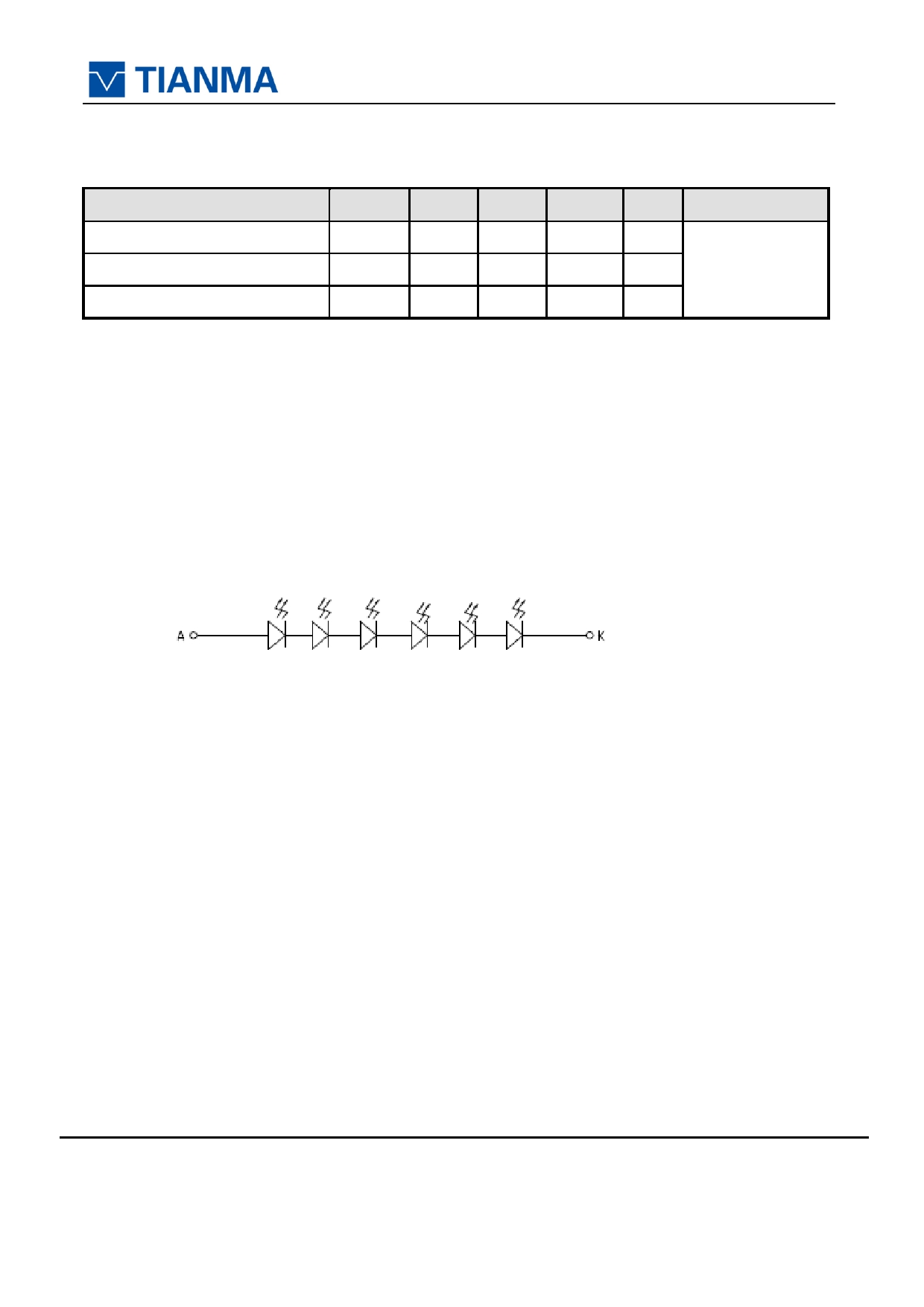
LED Numbers
6 LEDs Serial
Note 1: Requirements on Environmental Protection: Q/S0002
Note 2: LCM weight tolerance: ± 5%
The information contained herein is the exclusive property of TIANMA MICRO-ELECTRONICS
Corporation and shall not be distributed, reproduced, or disclosed in whole or in part without prior written
permission of TIANMA MICRO-ELECTRONICS Corporation.
Page 4 of 19
TM033XDHG01-00
2 Input/Output Terminals
2.1 TFT LCD Panel
No
Symbol
I/O
Description
1
GND
P
Ground
2
RST
I
Global reset signal
3
GND
P
Ground
4
MIPI_Data-N
I
MIPI Clock
5
MIPI_Data-P
I
MIPI Clock
6
GND
P
Ground
7
MIPI_CLK-N
I
MIPI Data
8
MIPI_CLK-P
I
MIPI Data
9
GND
P
Ground
10
TE
O
Tearing effect output
11
GND
P
Ground
12
VDD
P
Analog power supply
13
VDDIO
P
Digital power supply
14
GND
P
Ground
15
LEDA
P
LED Anode
16
LEDK
P
LED Cathode
17
GND
P
Ground
Note 1: I —— Input , O —— Output , P —— Power/Ground,VCC=VDD
Table 2.1 Terminal pin assignments
The information contained herein is the exclusive property of TIANMA MICRO-ELECTRONICS
Corporation and shall not be distributed, reproduced, or disclosed in whole or in part without prior written
permission of TIANMA MICRO-ELECTRONICS Corporation.
Page 5 of 19
TM033XDHG01-00
3 Absolute Maximum Ratings
3.1 Driving TFT LCD Panel
Ta =25 ℃
Item
Symbol
MIN
MAX
Unit
Remark
Power Supply Voltage
VDD
-0.3
4
V
Back Light Forward
Current
ILED
25
mA
One LED
Operating
Temperature
T OPR
-20
70
℃
Storage Temperature
T STG
-30
80
℃
--
≤ 95
%
Ta ≤ 40 ℃
--
≤ 85
%
40 ℃< Ta ≤ 50 ℃
Relative Humidity
Note2
RH
--
≤ 55
%
50 ℃< Ta ≤ 60 ℃
--
≤ 36
%
60 ℃< Ta ≤ 70 ℃
--
≤ 24
%
70 ℃< Ta ≤ 80 ℃
Absolute Humidity
AH
--
≤ 70
g/m ³
Ta > 70 ℃
Table 3.1 absolute maximum rating
Notes:
1. In case of below 0 ℃, the response time of liquid crystal (LC)becomes slower .
2. The color of panel becomes darker than normal one. Level of retardation depends on temperature,
because of LC's characteristics.
3. If the module is above these absolute maximum ratings. It may become permanently damaged.
Using the module within the following electrical characteristic conditions are also exceeded,
the module will malfunction and cause poor reliability.
The information contained herein is the exclusive property of TIANMA MICRO-ELECTRONICS
Corporation and shall not be distributed, reproduced, or disclosed in whole or in part without prior written
permission of TIANMA MICRO-ELECTRONICS Corporation.
Page 6 of 19
TM033XDHG01-00
4
E lectrical Characteristics
4.1 Driving TFT LCD Panel
GND=0V , Ta=25 ℃
Item
Symbol
MIN
TYP
MAX
Unit
Remark
Supply Voltage
VDD
2.5
2.8
3.6
V
Connect to
IO Supply Voltage
VDDI
1.65
2.8
VDD
V
VDD
internal.
Low
VIL
DGND
—
0.3 VDDI
V
Input Signal Level
Voltage
High
Level
VIH
0.7 VDDI
—
VDDI
V
Low
Output
Level
VOL
DGND
—
0.2VDDI
V
Signal
Voltage
High
Level
VOH
0.8VDDI
—
VDDI
V
Black Mode
(Panel+LSI)
(60Hz)
mA
Note 1,3,4
Power Consumption
Sleep Mode
mA
Note 3,4
Table 4.1 LCD module electrical characteristics
Notes:
1. All pixels black.
2. All pixels white.
3. Typical: VDDI=1.8V, VDD=2.8V; Maximum: VDDI=3.3V, VDD=3.3V
4.The power consumption was only reference
The information contained herein is the exclusive property of TIANMA MICRO-ELECTRONICS
Corporation and shall not be distributed, reproduced, or disclosed in whole or in part without prior written
permission of TIANMA MICRO-ELECTRONICS Corporation.
Page 7 of 19
TM033XDHG01-00
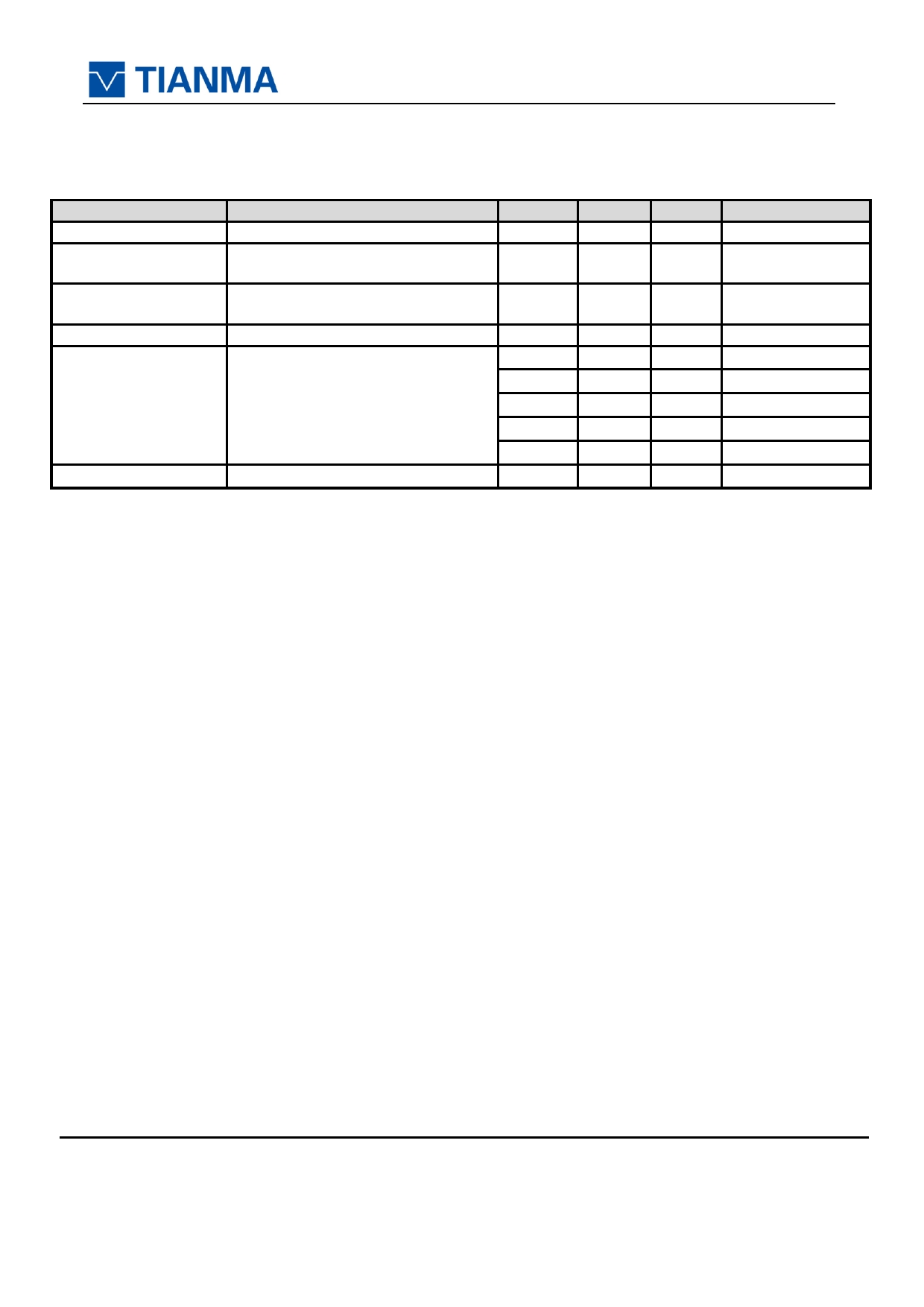
4.2 Backlight Unit
Ta=25 ℃
Item
Symbol
Min
Typ
Max
Unit
Remark
Forward Current
I F
18
20
25
mA
Forward Voltage
V F
16.8
18.0
19.2
V
6 LEDs
(6 LED Serial,)
Operating Life Time
-
20,000
-
-
Hrs
Note1: The LED driving condition is defined for each LED module (6 LED Serial,).For each
LED:
I F =20mA, V F (1/6) =3.2V.
Note2: Under LCM operating, the stable forward current should be inputted. And forward
voltage is for reference only.
Note3: I F is defined for one channel LED. Optical performance should be evaluated at
Ta=25 ℃ only If LED is driven by high current, high ambient temperature & humidity
condition. The life time of LED will be reduced. Operating life means brightness goes
down to 50% initial brightness. Typical operating life time is estimated data.
Note4: The LED driving condition is defined for each LED
The information contained herein is the exclusive property of TIANMA MICRO-ELECTRONICS
Corporation and shall not be distributed, reproduced, or disclosed in whole or in part without prior written
permission of TIANMA MICRO-ELECTRONICS Corporation.
Page 8 of 19
TM033XDHG01-00
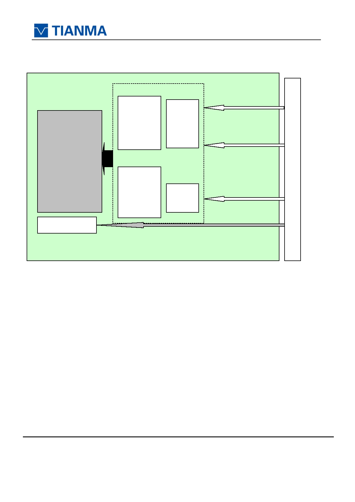
4.3 Block Diagram
LCD module diagram
MIPI Data
Data bus
VCOM
Source + Gate
&
Driver
TCON
MIPI CLK
3.34inch
320(RGB)*320
Control
signal input
Grayscale
Manipulation
Voltage
VDD,GND
DC/DC
Power
4.4 Input Setup Timing
LED- 、 LED+
BLU
BLU
The information contained herein is the exclusive property of TIANMA MICRO-ELECTRONICS
Corporation and shall not be distributed, reproduced, or disclosed in whole or in part without prior written
permission of TIANMA MICRO-ELECTRONICS Corporation.
Page 9 of 19

TM033XDHG01-00
5
Timing Chart
5.1 INTERFACE TIMING
5.2 Reset Timing
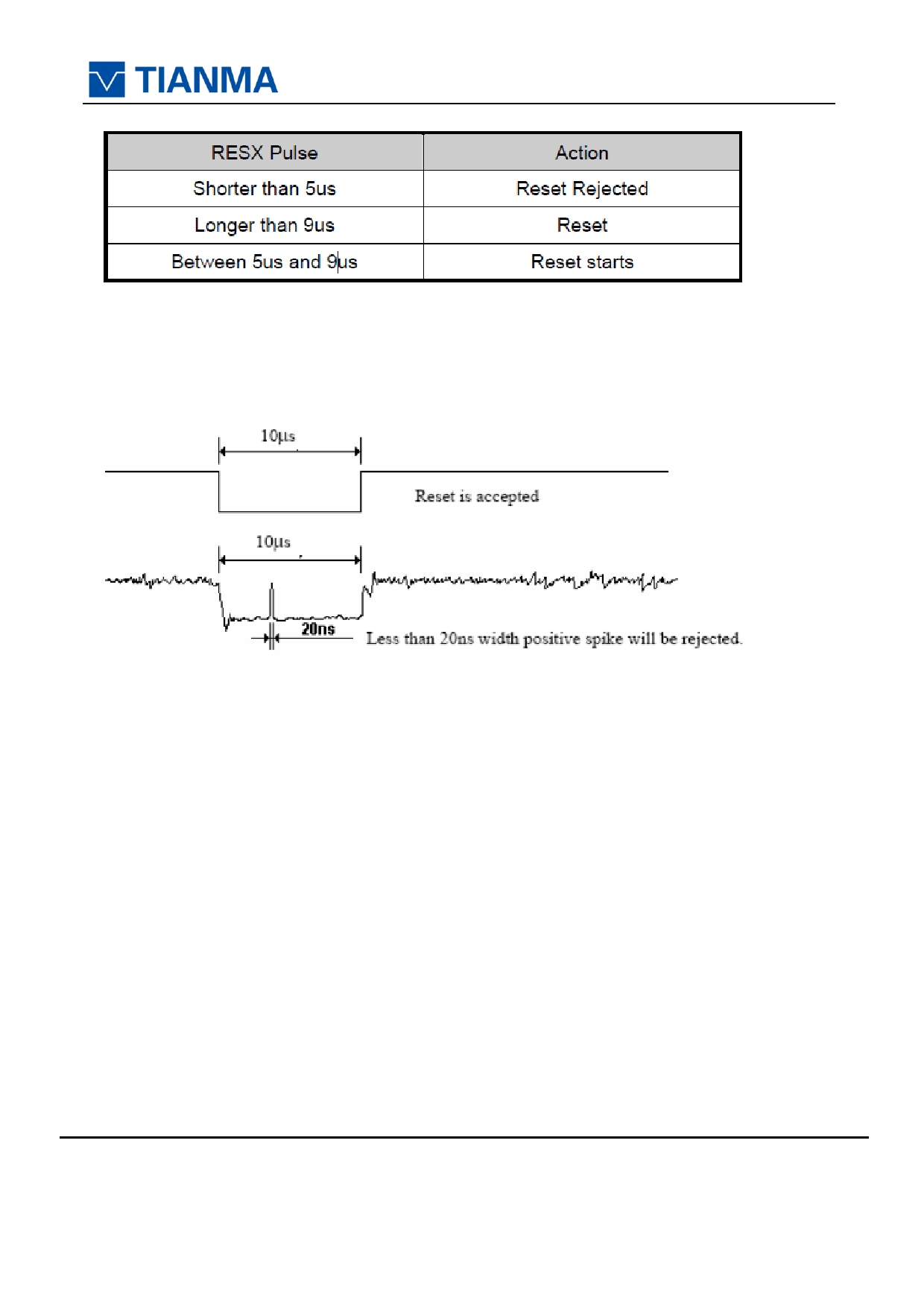
Notes:
1. The reset cancel includes also required time for loading ID bytes, VCOM setting and other settings from
NVM (or similar device) to
registers. This loading is done every time when there is HW reset cancel time (tRT) within 5 ms after a rising
edge of RESX.
2. Spike due to an electrostatic discharge on RESX line does not cause irregular system reset according to the
table below:
The information contained herein is the exclusive property of TIANMA MICRO-ELECTRONICS
Corporation and shall not be distributed, reproduced, or disclosed in whole or in part without prior written
permission of TIANMA MICRO-ELECTRONICS Corporation.
Page 10 of 19
TM033XDHG01-00
3. During the Resetting period, the display will be blanked (The display is entering blanking sequence, which
maximum time is 120
ms, when Reset Starts in Sleep Out – mode. The display remains the blank state in Sleep In – mode.) and then
return to Default condition
for Hardware Reset.
4. Spike Rejection also applies during a valid reset pulse as shown below:
5. When Reset applied during Sleep In Mode.
6. When Reset applied during Sleep Out Mode.
7. It is necessary to wait 5msec after releasing RESX before sending commands. Also Sleep Out command
cannot be sent for
120msec.
The information contained herein is the exclusive property of TIANMA MICRO-ELECTRONICS
Corporation and shall not be distributed, reproduced, or disclosed in whole or in part without prior written
permission of TIANMA MICRO-ELECTRONICS Corporation.
Page 11 of 19
TM033XDHG01-00
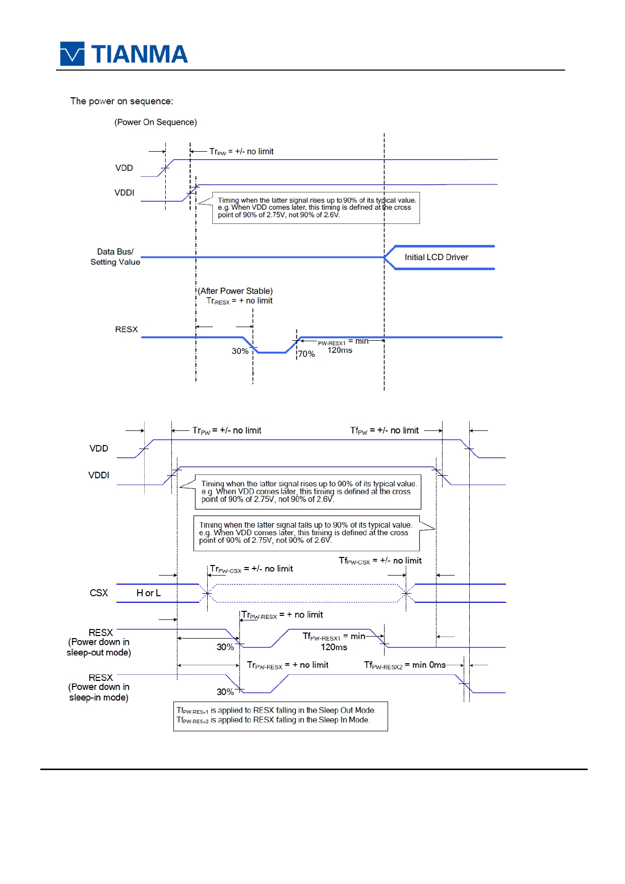
5. 3 Power-On Sequence
5. 4 Power-Off Sequence
Note: Please refer to ST7796SI data sheet for more details.ST7796SI INTERFACE PROTOCOL
The information contained herein is the exclusive property of TIANMA MICRO-ELECTRONICS
Corporation and shall not be distributed, reproduced, or disclosed in whole or in part without prior written
permission of TIANMA MICRO-ELECTRONICS Corporation.
Page 12 of 19
TM033XDHG01-00
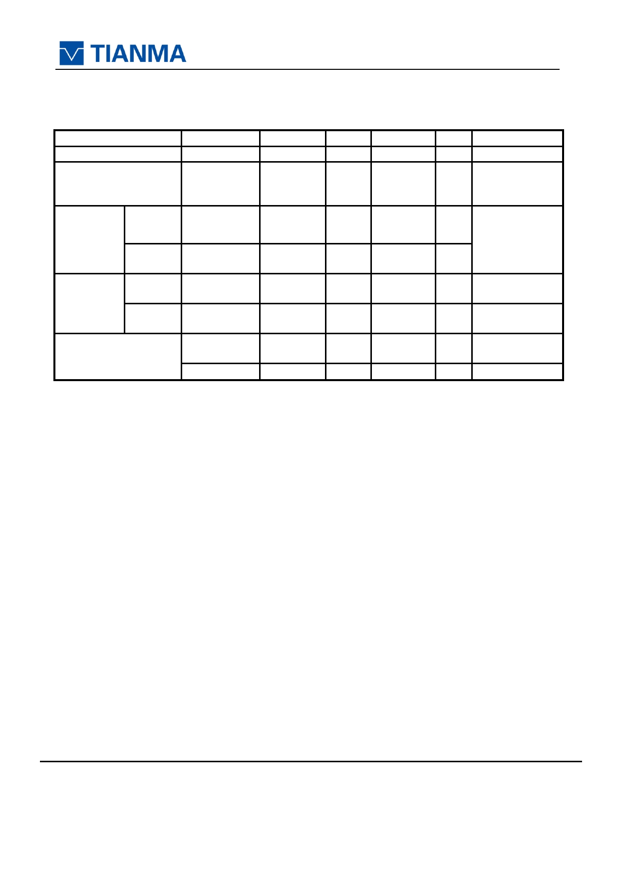
6 Optical Characteristics
Ta=25 ℃
Item
Symbol Condition
Min
Typ
Max
Unit
Remark
θT
60
70
-
θB
70
80
-
View Angles
CR≥10
Degree Note2,3
θL
70
80
-
θR
70
80
-
Contrast Ratio
CR
θ=0 o
600
800
-
Note 3
T ON
Response Time
25 ℃
-
20
30
ms
Note 4
T OFF
x
0.235
0.285
0.335
White
Note 1,5
y
0.258
0.308
0.358
x
0.535
0.585
0.635
Red
Note 1,5
y
0.274
0.324
0.374
Chromaticity
Backlight is
-
x
on
0.289
0.339
0.389
Green
Note 1,5
y
0.537
0.587
0.637
x
0.101
0.151
0.201
Blue
Note 1,5
y
0.038
0.088
0.138
Uniformity
U
70
75
-
%
Note 6
NTSC
45
50
-
%
Note 5
Luminance(without
2
lens)
L
600
-
-
cd/m
Note 7
Test Conditions:
1. I F = 20 mA, and the ambient temperature is 25 ℃ .
2. The test systems refer to Note 1 and Note 2.
The information contained herein is the exclusive property of TIANMA MICRO-ELECTRONICS
Corporation and shall not be distributed, reproduced, or disclosed in whole or in part without prior written
permission of TIANMA MICRO-ELECTRONICS Corporation.
Page 13 of 19
TM033XDHG01-00
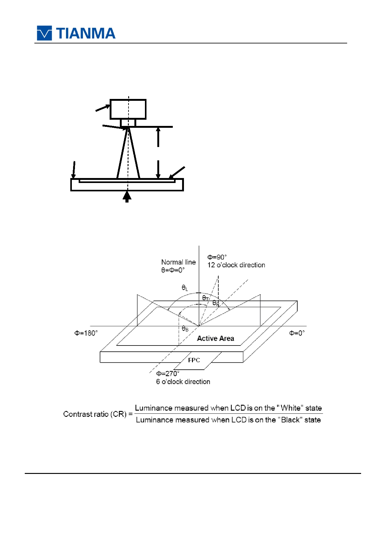
Note 1: Definition of optical measurement system.
The optical characteristics should be measured in dark room. After 5 Minutes operation, the optical
properties are measured at the center point of the LCD screen. All input terminals LCD panel must
be ground when measuring the center area of the panel.
Photo detector
Field
500mm
TFT-LCD Module
LCD Panel
The center of the screen
Note 2: Definition of viewing angle range and measurement system.
viewing angle is measured at the center point of the LCD by CONOSCOPE(ergo-80) 。
Note 3: Definition of contrast ratio
“White state “: The state is that the LCD should drive by Vwhite.
“Black state”: The state is that the LCD should drive by Vblack.
Vwhite: TBD V
Vblack: TBD V.
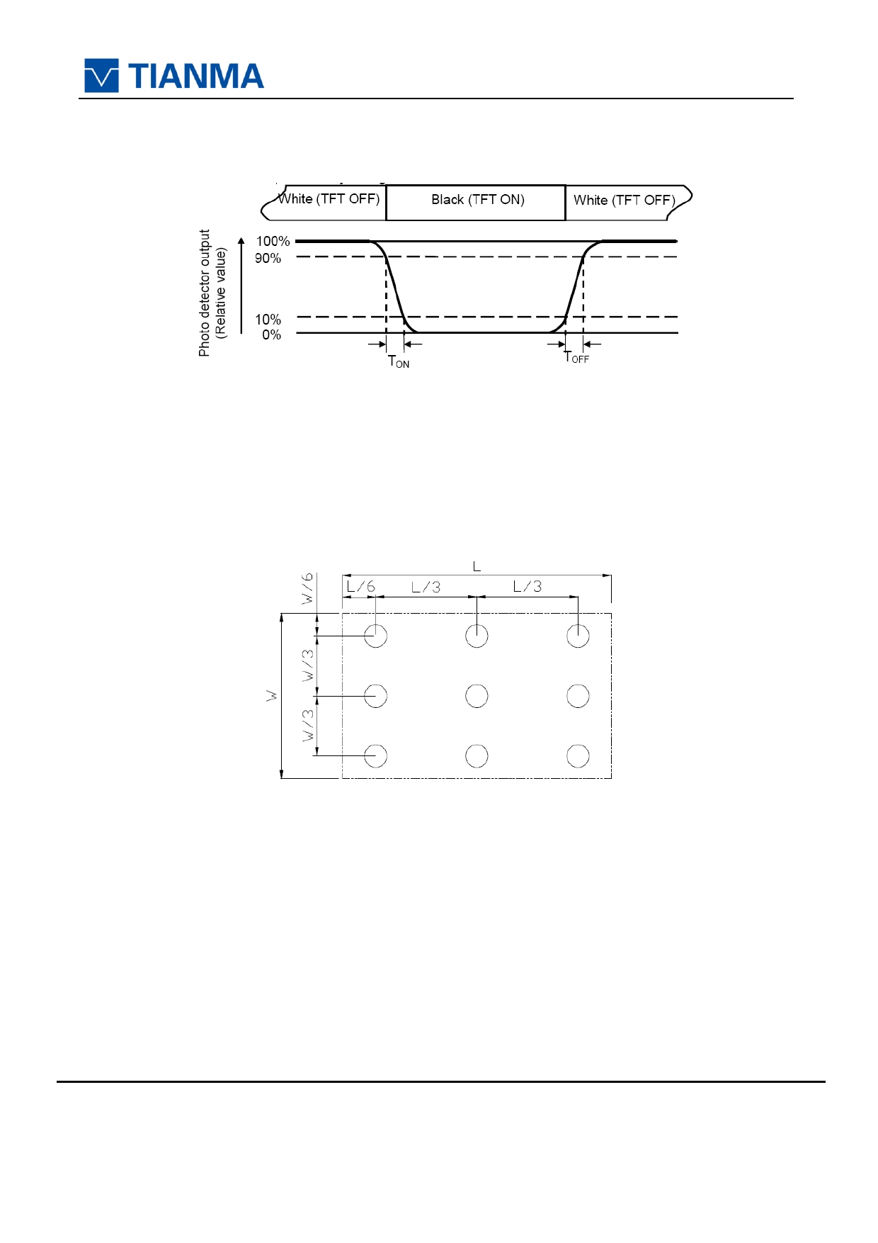
Note 4: Definition of Response time
The information contained herein is the exclusive property of TIANMA MICRO-ELECTRONICS
Corporation and shall not be distributed, reproduced, or disclosed in whole or in part without prior written
permission of TIANMA MICRO-ELECTRONICS Corporation.
Page 14 of 19
TM033XDHG01-00
The response time is defined as the LCD optical switching time interval between “White” state and
“Black” state. Rise time (T ON ) is the time between photo detector output intensity changed from 90%
to 10%. And fall time (T OFF ) is the time between photo detector output intensity changed from 10% to
90%.
Note 5: Definition of color chromaticity (CIE1931)
Color coordinates measured at center point of LCD.
Note 6: Definition of Luminance Uniformity
Active area is divided into 9 measuring areas (Refer Fig. 2). Every measuring point is placed at the
center of each measuring area.
Luminance Uniformity (U) = Lmin/ Lmax
L-------Active area length W----- Active area width
Lmax: The measured Maximum luminance of all measurement position.
Lmin: The measured Minimum luminance of all measurement position.
Note 7: Definition of Luminance:
Measure the luminance of white state at center point.
The information contained herein is the exclusive property of TIANMA MICRO-ELECTRONICS
Corporation and shall not be distributed, reproduced, or disclosed in whole or in part without prior written
permission of TIANMA MICRO-ELECTRONICS Corporation.
Page 15 of 19
TM033XDHG01-00
7 Environmental / Reliability Tests
No
Test Item
Condition
Remarks
1
High Temperature
Note1
Operation
Ts=+70 ℃ , 160hrs
IEC60068-2-1,GB2423.2
2
Low Temperature
IEC60068-2-1
Operation
Ta=-20 ℃ , 160hrs
GB2423.1
3
High Temperature
IEC60068-2-1
Storage
Ta=+80 ℃ , 160hrs
GB2423.2
4
Low Temperature
IEC60068-2-1
Storage
Ta=-30 ℃ , 160hrs
GB2423.1
High Temperature
Note2
5
& High Humidity
Ta=+60 ℃ , 90% RH
IEC60068-2-78
Storage
160 hours
GB/T2423.3
Start with cold temperature,
6
Thermal Shock
-20 ℃ 30 min ~ +60 ℃ 30 min,
(Non-operation)
Change time: 1min, 100 Cycles
End with high temperature,
IEC60068-2-14,GB2423.22
C=150pF, R=330Ω , 5points/panel
Electro Static
Air:±4KV, 5times;
IEC61000-4-2
7
Discharge
Contact:±2KV, 5 times;
GB/T17626.2
(Operation)
( Environment: 15 ℃ ~ 35 ℃ ,
Class B
30% ~ 60%, 86Kpa ~ 106Kpa )
Frequency range:10~55Hz,
Stroke:1.5mm
8
Package
Sweep:10Hz~55Hz~10Hz 2 hours
IEC60068-2-6
Vibration Test
for each direction of X.Y.Z.
GB/T2423.10
(6 hours for total)(Package
condition)
9
Shock
60G 6ms, ±X,±Y,±Z 3times,
IEC60068-2-27
(Non-operation)
for each direction
GB/T2423.5
10
Package
Height:60 cm,
IEC60068-2-32
Drop Test
1 corner, 3 edges, 6 surfaces
GB/T2423.8
Note1: Ts is the temperature of panel’s surface.
Note2: Ta is the ambient temperature of sample.
Note3: Before cosmetic and function test, the product must have enough recovery time, at least 2
hours at room temperature.
Note 4: In the standard condition, there shall be no practical problem that may affect the display
function. After the reliability test, the product only guarantees operation, but don ’t guarantee all of the
cosmetic specification.
The information contained herein is the exclusive property of TIANMA MICRO-ELECTRONICS
Corporation and shall not be distributed, reproduced, or disclosed in whole or in part without prior written
permission of TIANMA MICRO-ELECTRONICS Corporation.
Page 16 of 19
TM033XDHG01-00
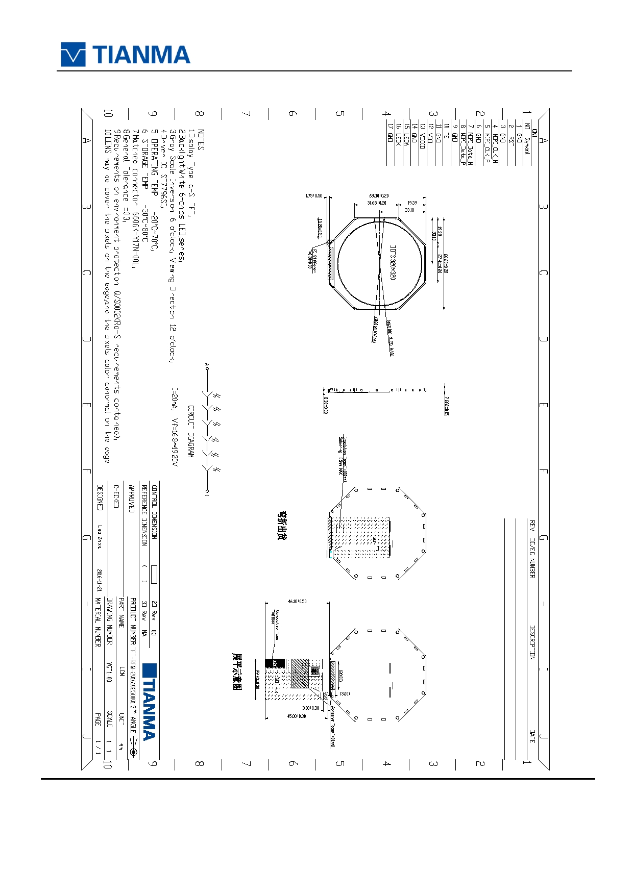
8 Mechanical Drawing
The information contained herein is the exclusive property of TIANMA MICRO-ELECTRONICS
Corporation and shall not be distributed, reproduced, or disclosed in whole or in part without prior written
permission of TIANMA MICRO-ELECTRONICS Corporation.
Page 17 of 19
TM033XDHG01-00
9 Packing Drawing
No
Item
Model (Material)
Dimensions(mm)
Unit
Weight(Kg)
Quantity
Remark
1
LCM module
TBD
126
2
Tray
TM033XDZN01-00
251×351×13.5
TBD
24
YBZ1-00
3
EPE1
MBZ-ZZML1
336×246×6mm
TBD
6
4
EPE2
MBZ-ZZM15
375×275×10mm
TBD
4
5
EPE3
MBZ-ZZM16
250×280×12mm
TBD
2
6
Carton
X18A
395×290×315mm
TBD
1
7
ES bag
JD13
400×520
TBD
3
8
Total weight
TBD±5% Kg
The information contained herein is the exclusive property of TIANMA MICRO-ELECTRONICS
Corporation and shall not be distributed, reproduced, or disclosed in whole or in part without prior written
permission of TIANMA MICRO-ELECTRONICS Corporation.
Page 18 of 19

TM033XDHG01-00
10 Precautions for Use of LCD Modules
10.1 Handling Precautions
10.1.1 The display panel is made of glass. Do not subject it to a mechanical shock by dropping it
from a high place, etc.
10.1.2 If the display panel is damaged and the liquid crystal substance inside it leaks out, be sure
not to get any in your mouth, if the substance comes into contact with your skin or clothes, promptly
wash it off using soap and water.
10.1.3 Do not apply excessive force to the display surface or the adjoining areas since this may
cause the color tone to vary.
10.1.4 The polarizer covering the display surface of the LCD module is soft and easily scratched.
Handle this polarizer carefully.
10.1.5 If the display surface is contaMinated, breathe on the surface and gently wipe it with a soft
dry cloth. If still not completely clear, moisten cloth with one of the following solvents:
- Isopropyl alcohol
- Ethyl alcohol
Solvents other than those mentioned above may damage the polarizer. Especially, do not use the
following:
- Ketone
- Aromatic solvents
10.1.6 Do not attempt to disassemble the LCD Module.
10.1.7 If the logic circuit power is off, do not apply the input signals.
10.1.8 To prevent destruction of the elements by static electricity, be careful to maintain an optimum
work environment.
10.1.8.1 Be sure to ground the body when handling the LCD Modules.
10.1.8.2 Tools required for assembly, such as soldering irons, must be properly ground.
10.1.8.3 To reduce the amount of static electricity generated, do not conduct assembly and other
work under dry conditions.
10.1.8.4 The LCD Module is coated with a film to protect the display surface. Be care when
peeling off this protective film since static electricity may be generated.
10.2 Storage precautions
10.2.1
When storing the LCD modules, avoid exposure to direct sunlight or to the light of
fluorescent lamps.
10.2.2 The LCD modules should be stored under the storage temperature range. If the LCD
modules will be stored for a long time, the recommend condition is:
Temperature : 0 ℃ ~ 40 ℃ Relatively humidity: ≤80%
10.2.3 The LCD modules should be stored in the room without acid, alkali and harmful gas.
10.3
Transportation Precautions
10.3.1 The LCD modules should be no falling and violent shocking during transportation, and also
should avoid excessive press, water, damp and sunshine.
The information contained herein is the exclusive property of TIANMA MICRO-ELECTRONICS
Corporation and shall not be distributed, reproduced, or disclosed in whole or in part without prior written
permission of TIANMA MICRO-ELECTRONICS Corporation.
Page 19 of 19