TM084SDHG02
MODEL NO
:
TM084SDHG02
MODEL VERSION:
00
SPEC VERSION :
2.2
ISSUED DATE:
2015-11-25
□Preliminary Specification
■Final Product Specification
Customer :
Approved by
Notes
TIANMA Confirmed :
Prepared by
Checked by
Approved by
Gang.li
Longping.Deng
Feng.Qin
This technical specification is subjected to change without prior notice.
The information contained herein is the exclusive property of SHANGHAI TIANMA OPTOELECTRONICS
Corporation, and shall not be distributed, reproduced, or disclosed in whole or in part without prior written
permission of SHANGHAI TIANMA OPTOELECTRONICS Corporation.
Page 1 of 20

TM084SDHG02
Table of Contents
Table of Contents ............................................................................................................................ 1
Record of Revision ......................................................................................................................... 3
1
General Specifications ............................................................................................................. 4
2
Input/Output Terminals ............................................................................................................. 5
3
Absolute Maximum Ratings ...................................................................................................... 6
4
Electrical Characteristics .......................................................................................................... 8
5
Timing Chart .......................................................................................................................... 10
6
Optical Characteristics ........................................................................................................... 14
7
Environmental / Reliability Test ............................................................................................... 17
8
Mechanical Drawing ............................................................................................................... 18
9
Packing drawing ..................................................................................................................... 19
10 Precautions for Use of LCD Modules ..................................................................................... 20
The information contained herein is the exclusive property of SHANGHAI TIANMA OPTOELECTRONICS
Corporation, and shall not be distributed, reproduced, or disclosed in whole or in part without prior written
permission of SHANGHAI TIANMA OPTOELECTRONICS Corporation.
Page 2 of 20

TM084SDHG02
Record of Revision
Rev
Issued Date
Description
Editor
1.0
2014-10-14 Preliminary Specification released.
Gang.li
2.0
2015-01-06 Modify FPC shape and dimension.
Gang.li
2.1
2015-05-20
Add copper clad on FPC bending area.
Gang.li
Add temperature and relative humidity descriptions on
2.2
2015-11-25 page7.
Gang.li
Final specification released.
The information contained herein is the exclusive property of SHANGHAI TIANMA OPTOELECTRONICS
Corporation, and shall not be distributed, reproduced, or disclosed in whole or in part without prior written
permission of SHANGHAI TIANMA OPTOELECTRONICS Corporation.
Page 3 of 20

TM084SDHG02
1 General Specifications
Feature
Spec
Size
8.4 inch
Resolution
800(RGB) x 600
Technology Type
a-Si TFT
Pixel Configuration
R.G.B. Vertical Stripe
Display Spec.
Pixel pitch(mm)
0.213 × 0.213
Display Mode
Transmissive, Normally white
Surface Treatment
Anti-Glare
Viewing Direction
12 o ’ clock
Gray Scale Inversion Direction
6 o ’ clock
LCM (W x H x D) (mm)
189.75x 149.4 x 4.8
Active Area(mm)
170.4 (W) X127.8(H)
With /Without TSP
Without TSP
Mechanical
Characteristics
Matching Connection Type(CN1)
FH28-60S-0.5SH(Hirose)
Matching Connection Type(CN2)
BHSR-02VS-1
LED Numbers
27 LEDS
Weight (g)
245
Interface
TTL(RGB 24bit)
Electrical
Characteristics
Color Depth
16.7M
Driver IC
NT51008B*2+NT52002*1
Note 1: Viewing direction for best image quality is different from TFT definition. There is a 180 degree
shift.
Note 2: Requirements on Environmental Protection: Q/S0002
Note 3: LCM weight tolerance: +/- 5%
The information contained herein is the exclusive property of SHANGHAI TIANMA OPTOELECTRONICS
Corporation, and shall not be distributed, reproduced, or disclosed in whole or in part without prior written
permission of SHANGHAI TIANMA OPTOELECTRONICS Corporation.
Page 4 of 20
TM084SDHG02
2 Input/Output Terminals
2.1 CN1 of FPC
Matched Connector type: FH28-60S-0.5SH(Hirose)
Pin
Symbol
I/O
Description
Remark
1
GND
P
Ground
2
NC
-
No connection
3
VCC
P
Power supply
4
R0
I
Red data Input(LSB)
5
R1
I
Red data Input
6
R2
I
Red data Input
7
R3
I
Red data Input
8
R4
I
Red data Input
9
R5
I
Red data Input
10
R6
I
Red data Input
11
R7
I
Red data Input(MSB)
12
G0
I
Green data Input(LSB)
13
G1
I
Green data Input
14
G2
I
Green data Input
15
G3
I
Green data Input
16
G4
I
Green data Input
17
G5
I
Green data Input
18
G6
I
Green data Input
19
G7
I
Green data Input(MSB)
20
B0
I
Blue data Input(LSB)
21
B1
I
Blue data Input
22
B2
I
Blue data Input
23
B3
I
Blue data Input
24
B4
I
Blue data Input
25
B5
I
Blue data Input
26
B6
I
Blue data Input
27
B7
I
Blue data Input(MSB)
28
DCLK
I
Clock input(L atch data at falling edge )
29
DE
I
Data enable
30
HSYNC
I
Horizontal sync input. Negative polarity
31
VSYNC
I
Vertical sync input. Negative polarity
32
MODE3
I
DE/SYNC mode select .normally pull high
H:DE mode .L:HV mode
Global reset pin. RSTB= “ 0 ” ,module reset;
33
RSTB
I
RSTB= “ 1 ” normal operation
Standby mode, normally pull high
34
STBYB
I
STBYB="1",normal operation
STBYB="0",source driver will turn off, all output are high-Z
Source right or left sequence control,normally pull high
35
SHLR
I
SHLR="L", shift left: last data=S1<-S2 … S1200=first data ;
SHLR="H", shift right :first data=S1->S2 … S1200=last data
36
VCC
P
Power supply
The information contained herein is the exclusive property of SHANGHAI TIANMA OPTOELECTRONICS
Corporation, and shall not be distributed, reproduced, or disclosed in whole or in part without prior written
permission of SHANGHAI TIANMA OPTOELECTRONICS Corporation.
Page 5 of 20

TM084SDHG02
Gate up or down scan control. Normally pull low
37
UPDN
I
UPDN="L" , DOWN shift :G1->G2 … ->G600 ;
UPDN="H", up shift: G1<-G2 … <-G600
38
GND
P
Ground
39
GND
P
Ground
40
NC
-
No connection
41
NC
-
No connection
Dithering setting
42
DITH
I
DITH="H" 6bit resolution (last 2 bits of input data truncated,
default setting)
DITH="L" 8bit resolution
43
NC
-
No connection
44
NC
-
No connection
45
NC
-
No connection
46
NC
-
No connection
47
NC
-
No connection
48
NC
-
No connection
49
NC
-
No connection
50
NC
-
No connection
51
NC
-
No connection
52
NC
-
No connection
53
NC
-
No connection
54
NC
-
No connection
55
NC
-
No connection
56
NC
-
No connection
57
NC
-
No connection
58
NC
-
No connection
59
GND
P
Ground
60
NC
-
No connection
I---Input, O---Output, P--- Power/Ground, “ - ” ---No connection
Table 2.1 terminal pin assignments
2.2 CN2 pin assignment (Backlight interface)
Mating Connector: SBHT-002T-P0.5 or equivalent
Pin
Symbol
I/O
Description
Remark
1
LED+(Anode)
P
LED power supply (high voltage)
2
LED-(Cathode)
P
LED power supply (low voltage)
Table 2.2 Backlight terminal pin assignments
The information contained herein is the exclusive property of SHANGHAI TIANMA OPTOELECTRONICS
Corporation, and shall not be distributed, reproduced, or disclosed in whole or in part without prior written
permission of SHANGHAI TIANMA OPTOELECTRONICS Corporation.
Page 6 of 20

TM084SDHG02
3 Absolute Maximum Ratings
GND=0V, Ta = 25 ℃
Item
Symbol
MIN
MAX
Unit
Remark
Power Voltage
VCC
-0.5
5.0
V
Data Input voltage
V IN
-0.5
5.0
V
Note1
Backlight forward current
I LED
-
30
mA
For each LED
Operating Temperature
Top
-20
70
℃
Storage Temperature
Tst
-30
80
℃
--
≤ 95
%
Ta ≤ 40 ℃
--
≤ 85
%
40 ℃< Ta ≤ 50 ℃
Relative Humidity
(Note2)
RH
--
≤ 55
%
50 ℃< Ta ≤ 60 ℃
--
≤ 36
%
60 ℃< Ta ≤ 70 ℃
--
≤ 24
%
70 ℃< Ta ≤ 80 ℃
Absolute Humidity
AH
--
≤ 70
g/m ³
Ta > 70 ℃
Table 3.1 absolute maximum rating
Note1: Signals input include Rx,Gx,Bx,DCLK,DE,HSYNC,VSYNC,MODE3,RSTB,STBYB,SHLR,
DITH.
Note2: Ta means the ambient temperature.
It is necessary to limit the relative humidity to the specified temperature range.
Condensation on the module is not allowed.
The information contained herein is the exclusive property of SHANGHAI TIANMA OPTOELECTRONICS
Corporation, and shall not be distributed, reproduced, or disclosed in whole or in part without prior written
permission of SHANGHAI TIANMA OPTOELECTRONICS Corporation.
Page 7 of 20

TM084SDHG02
4 Electrical Characteristics
4.1 Recommended Operating Condition
VCC=3.3V , GND=0V , Ta = 25 ℃
Item
Symbol
Min
Typ
Max
Unit
Remark
Supply Voltage
VCC
3.0
3.3
3.6
V
Input Signal Low Level
V B IL B
0
--
0.3xVCC
V
Voltage
High Level
V B IH B
0.7xVCC
--
VCC
V
Output
Low Level
V B OL B
--
--
GND+0.4
V
Signal
Voltage
High Level
V B OH B
VCC-0.4
--
--
V
(Panel+LSI)
Black Mode (60Hz)
--
660
--
mW
Note1
Power Consumption
Standby Mode
--
400
--
mW
Table 4.1 LCD module electrical characteristics
Note1: To test the current dissipation, use “ all Black Pattern ” .
4.2 Backlight Unit Driving Condition
LED_GND=GND=0V, Ta = 25 ℃
Item
Symbol
Min
Typ
Max
Unit
Remark
Channel1
I B F B
-
180
225
mA
Note 1
Forward Voltage
V B F B
9
9.6
10.8
V
Backlight Power Consumption
W B BL B
-
1728
-
mW
Life Time
-
-
30,000
-
Hrs
Note 3
Table 4.2 LED backlight characteristics
Note 1: If LED is driven by high current, high ambient temperature & humidity condition. The life time
of LED will be reduced. Operating life means brightness goes down to 50% initial brightness.
Typical operating life time is an estimated data.
Figure4.2 LED connection of backlight
The information contained herein is the exclusive property of SHANGHAI TIANMA OPTOELECTRONICS
Corporation, and shall not be distributed, reproduced, or disclosed in whole or in part without prior written
permission of SHANGHAI TIANMA OPTOELECTRONICS Corporation.
Page 8 of 20

TM084SDHG02
4.3 BLOCK DIAGRAM
LCD Panel
R[7:0] 、 G[7:0] 、 B[7:0]
Data
VCOM
bus
Source + Gate
&
Driver
TCON
VSYNC 、 HSYNC 、
8.4 inch
DE 、 DCLK 等
800(RGB)*600
Control
signal input
Grayscale
Manipulation
Voltage
Vcc 、 GND
DC/DC
Power
VLED+ 、 VLED-
BLU
BLU
The information contained herein is the exclusive property of SHANGHAI TIANMA OPTOELECTRONICS
Corporation, and shall not be distributed, reproduced, or disclosed in whole or in part without prior written
permission of SHANGHAI TIANMA OPTOELECTRONICS Corporation.
Page 9 of 20

TM084SDHG02
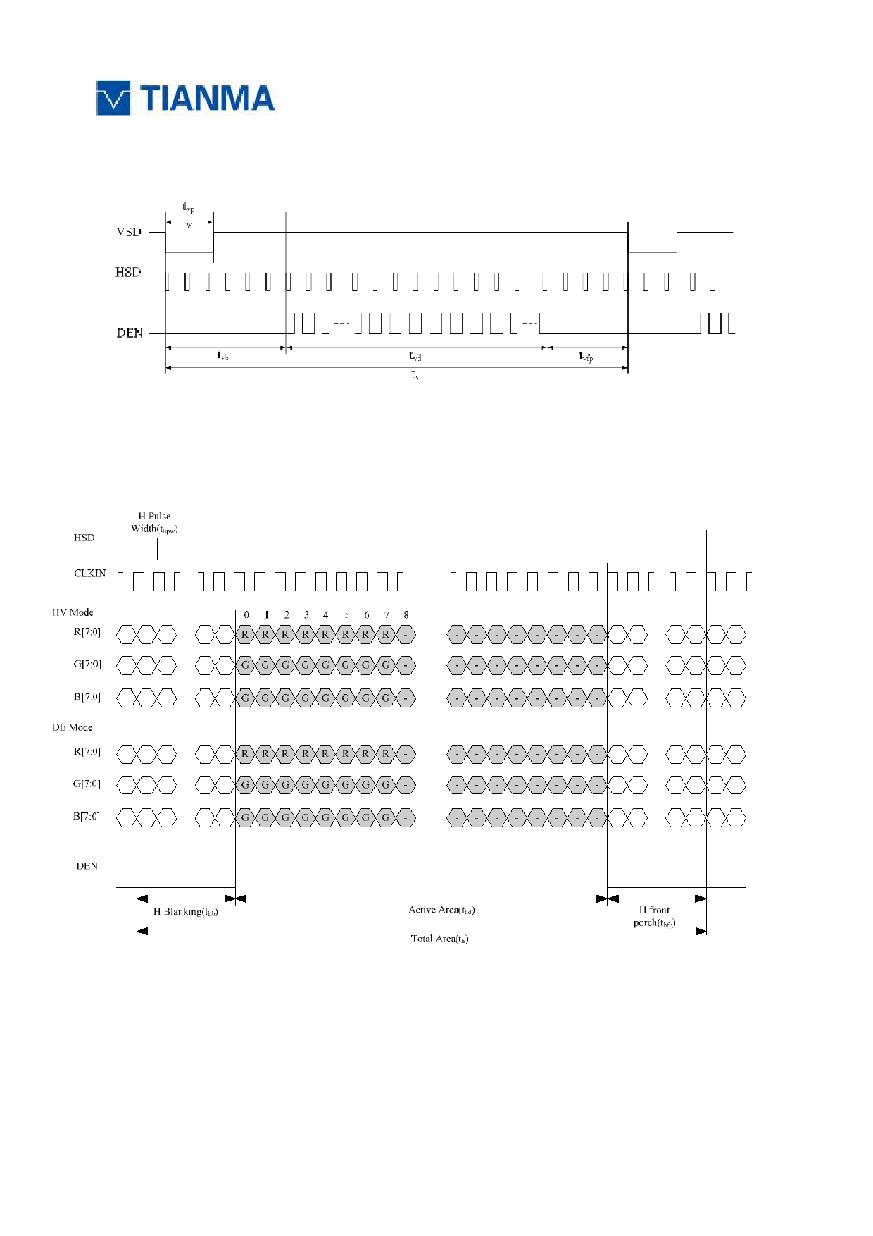
5 Timing Chart
5.1.1 AC characteristics
VCC=3.3V, GND=0V, Ta=25 ℃
Parameter
Symbol
Min
Typ
Max
Unit
Remark
HSYNC Setup Time
T B hst B
8
-
-
ns
HSYNC Hold Time
T B hhd B
8
-
-
ns
VSYNC Setup Time
T B vst B
8
ns
VSYNC Hold Time
T B vhd B
8
-
-
ns
Data Setup Time
T B dsu B
8
ns
Data Hold Time
T B dhd B
8
-
-
ns
DE Setup Time
T B esu B
8
-
-
ns
DE Hold Time
T B ehd B
8
-
-
ns
CLKIN Cycle Time
T B cph B
14
-
-
ns
CLKIN Pulse Width
T B cwh B
40
50
60
%
Output stable time
Tsst
-
-
6
us
From 0V to 90%
VCC Power ON Slew rate
Tpor
-
-
20
ms
VCC
RSTB pulse width
TRst
50
-
-
us
DCLK = 65MHz
Table 5.1 AC characteristics
Figure 5.1 AC characteristics
The information contained herein is the exclusive property of SHANGHAI TIANMA OPTOELECTRONICS
Corporation, and shall not be distributed, reproduced, or disclosed in whole or in part without prior written
permission of SHANGHAI TIANMA OPTOELECTRONICS Corporation.
Page 10 of 20

TM084SDHG02
5.2
Data input timing
5.2.1 Input timing at DE mode
VCC=3.3V, GND=0V, Ta=25 ℃
Parameter
Symb
Min.
Typ.
Max.
Unit
Remark
ol
Dclk frequency(Frame rate=60HZ)
Fclk
33
39.6
60
MHz
Tclk=1/Fclk
Horizontal total
TH
890
1000
1300
Tclk
Horizontal
section
Horizontal blanking
THC
90
200
500
Tclk
Note1
Valid Data Width
THD
-
800
-
Tclk
Vertical total
TV
610
660
800
TH
Vertical
section
Vertical blanking
TVC
10
60
200
TH
Note1
Valid Data Width
TVD
-
600
-
TH
Table 5.2.1 input timing (DE mode)
5.2.2
Input timing at HV mode
VCC=3.3V, GND=0V, Ta=25 ℃
Parameter
Symb
Min.
Typ.
Max.
Unit
Remark
ol
Dclk frequency(Frame rate=60HZ)
Fclk
35
39.6
50
MHz
Tclk=1/Fclk
Horizontal pulse width THPW
1
-
40
Tclk
Horizontal total
TH
900
1000
1200
Tclk
Horizontal
section
Horizontal back porch
THB
88
88
88
Tclk
Horizontal front porch
THFP
12
112
312
Tclk
Valid Data Width
THD
-
800
-
Tclk
Vertical pulse width
TVPW
1
-
20
TH
Vertical total
TV
640
660
700
TH
Vertical
section
Vertical back porch
TVB
39
39
39
TH
Vertical front porch
TVFP
1
21
61
TH
Valid Data Width
TVD
-
600
-
TH
Table 5.2.2 input timing (HV mode)
Note1: THC=THB+THFP, TVC=TVB+TVFP, In HV mode, it is necessary to keep it in typical value.
The information contained herein is the exclusive property of SHANGHAI TIANMA OPTOELECTRONICS
Corporation, and shall not be distributed, reproduced, or disclosed in whole or in part without prior written
permission of SHANGHAI TIANMA OPTOELECTRONICS Corporation.
Page 11 of 20
TM084SDHG02
5.3
Data input Timing Diagram
5.3.1 Vertical Input Timing Diagram
Figure 5.3.1 Vertical Input Timing Diagram
5.3.2 Horizontal Input Timing Diagram
Figure5.3.2 Vertical Input Timing Diagram
The information contained herein is the exclusive property of SHANGHAI TIANMA OPTOELECTRONICS
Corporation, and shall not be distributed, reproduced, or disclosed in whole or in part without prior written
permission of SHANGHAI TIANMA OPTOELECTRONICS Corporation.
Page 12 of 20

TM084SDHG02
5.4
POWER ON/OFF SEQUENCE
Item
Symbol
Min
Typ
Max
Unit
Remark
VCC 3.3V to signal starting
Tp1
5
-
50
ms
VCC rising time
Tr
0.1
-
5
ms
Note1
Signal starting to backlight on
Tp2
150
-
-
ms
Signal off to VCC 0V
Tp3
5
-
50
ms
Backlight off to signal off
Tp4
150
-
-
ms
Table 5.4 POWER ON/OFF SEQUENCE
Note1: Tr means the time of input voltage rise from 10% to 90%.
Tp3
3.3V
Tp1
0V
VCC
Signal
Tp2
Tp4
Backlight
Figure5.4 Interface power on/off sequence
The information contained herein is the exclusive property of SHANGHAI TIANMA OPTOELECTRONICS
Corporation, and shall not be distributed, reproduced, or disclosed in whole or in part without prior written
permission of SHANGHAI TIANMA OPTOELECTRONICS Corporation.
Page 13 of 20

TM084SDHG02
6 Optical Characteristics
Ta=25 ℃
Item
Symbol Condition
Min
Typ
Max
Unit
Remark
θ T
50
60
-
θ B
60
70
-
View Angles
CR ≧ 10
Degree Note 2
θ L
60
70
-
θ R
60
70
-
Note1
Contrast Ratio
CR
θ =0 °
400
500
-
Note3
T ON
Note1
Response Time
25 ℃
-
20
30
ms
T OFF
Note4
x
0.260
0.310
0.360
White
y
0.280
0.330
0.380
x
0.551
0.601
0.651
Red
y
0.281
0.331
0.381
Note1
Chromaticity
Backlight is
x
on
0.307
0.357
0.407
Note5
Green
y
0.527
0.577
0.627
x
0.102
0.152
0.202
Blue
y
0.056
0.106
0.156
Note1
Uniformity
U
70
75
-
%
Note6
NTSC
-
50
-
%
Note 5
Luminance ( Without
2
Note1
L
280
350
-
cd/m
TP )
Note7
Test Conditions:
1. I F = 180 mA, V F =10.5 V and the ambient temperature is 25 ± 2 ℃ .humidity is 65 ± 7%
2. The test systems refer to Note 1 and Note 2.
The information contained herein is the exclusive property of SHANGHAI TIANMA OPTOELECTRONICS
Corporation, and shall not be distributed, reproduced, or disclosed in whole or in part without prior written
permission of SHANGHAI TIANMA OPTOELECTRONICS Corporation.
Page 14 of 20

TM084SDHG02
Note 1: Definition of optical measurement system.
The optical characteristics should be measured in dark room. After 5 Minutes operation, the optical
properties are measured at the center point of the LCD screen. All input terminals LCD panel must be
ground when measuring the center area of the panel.
Photo detector
Item
Photo detector
Field
Field
Contrast Ratio
Luminance
SR-3A
1 °
500mm
Chromaticity
TFT-LCD Module
LCD Panel
Lum Uniformity
Response Time
BM-7A
2 °
The center of the screen
Note
2: Definition of viewing angle range and measurement system.
viewing angle is measured at the center point of the LCD by CONOSCOPE(ergo-80) 。
Note 3: Definition of contrast ratio
“ White state “ : The state is that the LCD should drive by Vwhite.
“ Black state ” : The state is that the LCD should drive by Vblack.
The information contained herein is the exclusive property of SHANGHAI TIANMA OPTOELECTRONICS
Corporation, and shall not be distributed, reproduced, or disclosed in whole or in part without prior written
permission of SHANGHAI TIANMA OPTOELECTRONICS Corporation.
Page 15 of 20

TM084SDHG02
Vwhite: To be determined
Vblack: To be determined.
Note 4: Definition of Response time
The response time is defined as the LCD optical switching time interval between “ White ” state and “ Black ”
state. Rise time (T ON ) is the time between photo detector output intensity changed from 90% to 10%. And
fall time (T OFF ) is the time between photo detector output intensity changed from 10% to 90%.
Note 5: Definition of color chromaticity (CIE1931)
Color coordinates measured at center point of LCD.
Note 6: Definition of Luminance Uniformity
Active area is divided into 9 measuring areas (Refer Fig. 2). Every measuring point is placed at the center
of each measuring area.
Luminance Uniformity (U) = Lmin/ Lmax
L-------Active area length W----- Active area width
Lmax: The measured Maximum luminance of all measurement position.
Lmin: The measured Minimum luminance of all measurement position.
Note 7: Definition of Luminance:
Measure the luminance of white state at center point.
The information contained herein is the exclusive property of SHANGHAI TIANMA OPTOELECTRONICS
Corporation, and shall not be distributed, reproduced, or disclosed in whole or in part without prior written
permission of SHANGHAI TIANMA OPTOELECTRONICS Corporation.
Page 16 of 20

TM084SDHG02
7 Environmental / Reliability Test
No
Test Item
Condition
Remarks
1
High Temperature
IEC60068-2-1
Operation
Ts = +70 ℃ , 240 hours
GB2423.2
2
Low Temperature
IEC60068-2-1
Operation
Ta = -20 ℃ , 2 40 hours
GB2423.1
3
High Temperature
IEC60068-2-1
Storage
Ta = +80 ℃ , 240 hours
GB2423.2
4
Low Temperature
IEC60068-2-1
Storage
Ta = -30 ℃ , 240 hours
GB2423.1
Storage at High
5
Temperature and Ta = +60 ℃ , 90% RH max,240hours
IEC60068-2-78
Humidity
GB/T2423.3
Start with cold temperature,
6
Thermal Shock
-30 ℃ 30 min~+80 ℃ 30 min,
(non-operation)
End with high temperature,
Change time:5min, 100 Cycle
IEC60068-2-14,GB2423.22
C=150pF,R=330 Ω ,5point/panel
Air: ± 8Kv,5times;
7
ESD
Contact: ± 4Kv,5times
IEC61000-4-2
(Environment:15 ℃ ~35 ℃ ,
GB/T17626.2
30%~60%.86Kpa~106Kpa)
Frequency range:10~55Hz
Stroke:1.5mm
8
Vibration Test
Sweep:10Hz~55Hz~10Hz
IEC60068-2-6
2 hours for each direction of X.Y.Z.
GB/T2423.10
(6 hours for total)
Half Sine Wave
9
Mechanical Shock
IEC60068-2-27
(Non Op)
60G 6ms, ± X, ± Y, ± Z
3times for each direction
GB/T2423.5
10
Package Drop
Height:60cm,
IEC60068-2-32
Test
1corner,3edges,6surfaces
GB/T2423.8
Note1: Ts is the temperature of panel ’ s surface.
Note2: Ta is the ambient temperature of samples.
The information contained herein is the exclusive property of SHANGHAI TIANMA OPTOELECTRONICS
Corporation, and shall not be distributed, reproduced, or disclosed in whole or in part without prior written
permission of SHANGHAI TIANMA OPTOELECTRONICS Corporation.
Page 17 of 20

TM084SDHG02
8 Mechanical Drawing
The information contained herein is the exclusive property of SHANGHAI TIANMA OPTOELECTRONICS
Corporation, and shall not be distributed, reproduced, or disclosed in whole or in part without prior written
permission of SHANGHAI TIANMA OPTOELECTRONICS Corporation.
Page 18 of 20

TM084SDHG02
9 Packing drawing
Unit
No.
Item
Model (Material)
Dimensions(mm)
Weight(Kg)
Quantity
Remark
1
LCM module
TM084SDHG02-00
189.75X149.4X4.8
0.245
36
2
Partition_1
Corrugated paper
527X348X217
1.571
1
3
Anti-static Bag
PE
161X253X0.05
0.001
36
Anti-static
4
Dust-Proof Bag
PE
700X545
0.06
1
5
Partition_2
Corrugated Paper
505X332X4.0
0.092
2
6
Corrugated Bar
Corrugated paper
348X173
0.057
4
7
Carton
Corrugated paper
544X365X250
0.76
1
8
Beauty-grain
Beauty-grain
30x10
0.001
2
9
Label
label
100x52
0.001
1
10
Total weight
11.66 ± 5%) kg
Table 9: Packing specification and quantity
Figure 9: Packing instruction
The information contained herein is the exclusive property of SHANGHAI TIANMA OPTOELECTRONICS
Corporation, and shall not be distributed, reproduced, or disclosed in whole or in part without prior written
permission of SHANGHAI TIANMA OPTOELECTRONICS Corporation.
Page 19 of 20

TM084SDHG02
10 Precautions for Use of LCD Modules
10.1 Handling Precautions
10.1.1
The display panel is made of glass. Do not subject it to a mechanical shock by dropping it
from a high place, etc.
10.1.2
If the display panel is damaged and the liquid crystal substance inside it leaks out, be sure not
to get any in your mouth, if the substance comes into contact with your skin or clothes, promptly wash it off
using soap and water.
10.1.3
Do not apply excessive force to the display surface or the adjoining areas since this may
cause the color tone to vary.
10.1.4
The polarizer covering the display surface of the LCD module is soft and easily scratched.
Handle this polarizer carefully.
10.1.5
If the display surface is contaminated, breathe on the surface and gently wipe it with a soft dry
cloth. If still not completely clear, moisten cloth with one of the following solvents:
- Isopropyl alcohol
- Ethyl alcohol
Solvents other than those mentioned above may damage the polarizer. Especially, do not use the
following:
- Water
- Ketone
- Aromatic solvents
10.1.6
Do not attempt to disassemble the LCD Module.
10.1.7
If the logic circuit power is off, do not apply the input signals.
10.1.8
To prevent destruction of the elements by static electricity, be careful to maintain an optimum
work environment.
10.1.8.1 Be sure to ground the body when handling the LCD Modules.
10.1.8.2 Tools required for assembly, such as soldering irons, must be properly ground.
10.1.8.3 To reduce the amount of static electricity generated, do not conduct assembly and other
work under dry conditions.
10.1.8.4 The LCD Module is coated with a film to protect the display surface. Be care when peeling
off this protective film since static electricity may be generated.
10.2 Storage precautions
10.2.1
When storing the LCD modules, avoid exposure to direct sunlight or to the light of fluorescent
lamps.
10.2.2
The LCD modules should be stored under the storage temperature range. If the LCD modules
will be stored for a long time, the recommend condition is 0 ℃ ~ 40 ℃ ,Relatively humidity: ≤ 80%
10.2.3
The LCD modules should be stored in the room without acid, alkali and harmful gas.
10.3 Transportation Precautions
10.3.1
The LCD modules should be no falling and violent shocking during transportation, and also
should avoid excessive press, water, damp and sunshine.
The information contained herein is the exclusive property of SHANGHAI TIANMA OPTOELECTRONICS
Corporation, and shall not be distributed, reproduced, or disclosed in whole or in part without prior written
permission of SHANGHAI TIANMA OPTOELECTRONICS Corporation.
Page 20 of 20