LM24064JFW
LCD Module User Manual
Prepared by:
Checked by:
Approved by:
Li KeKe
Date: 2021-04-19
Date:
Date:
Rev. Descriptions
Release Date
0.1
Preliminary release
2013-05-10
0.2
Add MTBF value,LED Backlight Life Time and Contrast Ratio.
2013-05-14
0.3
Change the outline demision and Update the AC characteristics.
2014-02-16
0.4
Update 1.4 and add outline drawing
2021-04-19
URL: www.topwaydisplay.com
Document Name: LM24064JFW-Manual-Rev.0.4
www.topwaysz.com
Page: 1 of 17

TOPWAY
LCD Module User Manual
LM24064JFW
Table of Content
1. Basic Specifications ............................................................................................................................. 3
1.1
Display Specifications .............................................................................................................................................................. 3
1.2
Mechanical Specifications ....................................................................................................................................................... 3
1.3
Block Diagram ........................................................................................................................................................................... 3
1.4
Terminal Functions(FPC) ........................................................................................................................................................ 4
1.5
Blacklight Terminal ................................................................................................................................................................... 4
2. Absolute Maximum Ratings ................................................................................................................ 5
3. Electrical Characteristics ..................................................................................................................... 5
3.1
DC Characteristics ................................................................................................................................................................... 5
3.2
LED Backlight Circuit Characteristics ................................................................................................................................... 5
3.3
AC Characteristics ................................................................................................................................................................... 6
3.4
Reset Timing ............................................................................................................................................................................. 8
4. Optical Characteristics ......................................................................................................................... 9
4.1
Optical Characteristics ............................................................................................................................................................. 9
4.2
Definition .................................................................................................................................................................................... 9
5. Function Specifications ..................................................................................................................... 11
5.1
Adjusting the Display Contrast ............................................................................................................................................. 11
5.2
Resetting the LCD module ................................................................................................................................................... 11
5.3
Application circuit (Example) ................................................................................................................................................ 11
5.4
Display Memory Map ............................................................................................................................................................. 12
5.5
Commands .............................................................................................................................................................................. 13
5.6
Command Table ..................................................................................................................................................................... 16
6. Design and Handling Precaution ..................................................................................................... 17
URL: www.topwaydisplay.com
Document Name: LM24064JFW-Manual-Rev.0.4
www.topwaysz.com
Page: 2 of 17
TOPWAY
LCD Module User Manual
LM24064JFW
1. Basic Specifications
1.1 Display Specifications
1) LCD Display Mode
: STN,Blue,Negative, Transmissive
2) Display Color
: Display Data = “1” : Light Gray (*1)
: Display Data = “0” : Dark Gray (*2)
3) Viewing Angle
: 6H
4) Driving Method
: 1/64 duty, 1/10 bias
5) Back Light
: White LED backlight
Note:
*1. Color tone may slightly change by Temperature and Driving Condition.
*2. The Color is defined as the inactive / background color
*3. Fine Contrast adjustment function is necessary in the application design for optimal display result
1.2 Mechanical Specifications
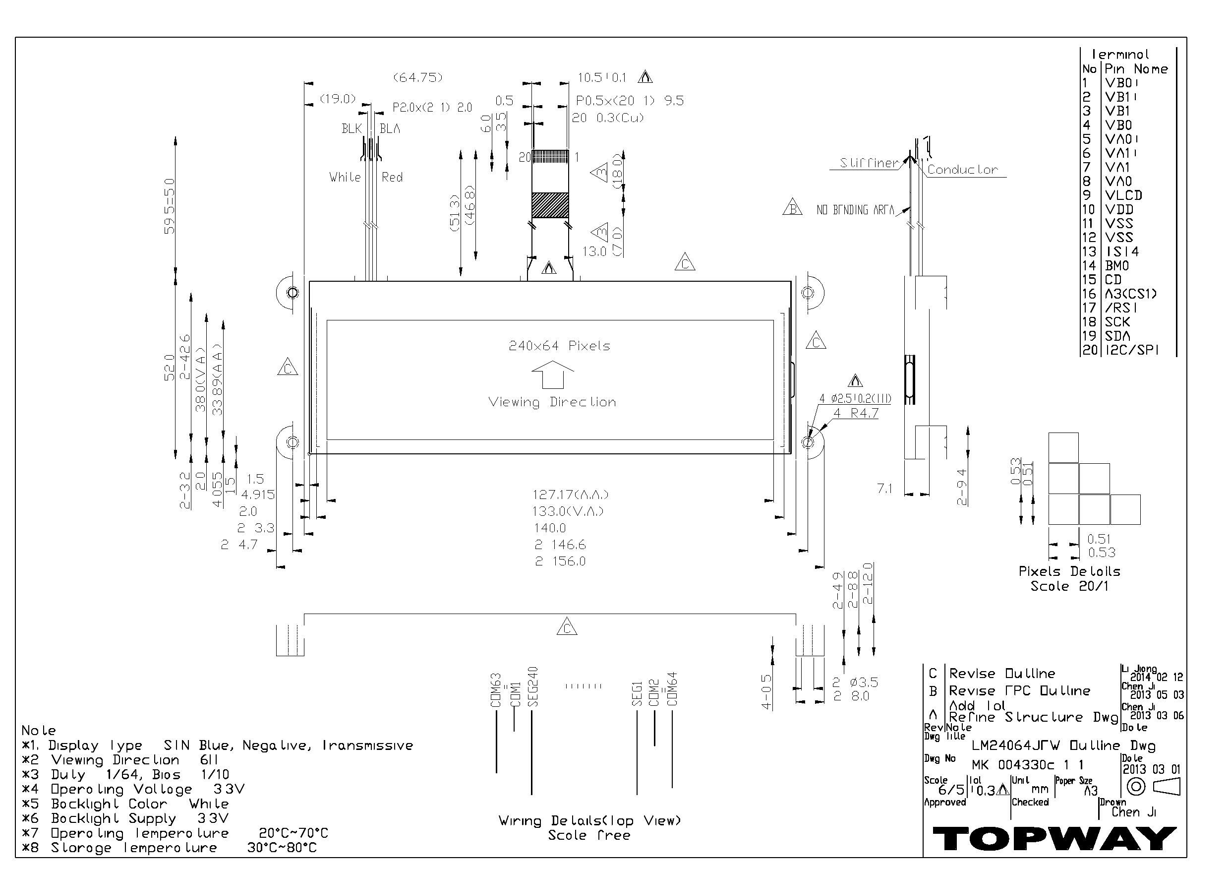
1) Outline Dimension
: 156.0x 52.0 x 12.0 (Exclude FPC)
(See attached Outline Drawing for details)
1.3 Block Diagram
LCD Panel
240 x 64 pixels
I2C/SPI,SDA,SCK,/RST
UC1611S
A3(CS1),CD,BM0,TST4
VLCD
or
VA0 -, VA1-,VA1+,VA0+
equivalent
VB0-,VB1-,VB1+,VB0+
VDD,VSS
BLA
Back Light Circuit
BLK
URL: www.topwaydisplay.com
Document Name: LM24064JFW-Manual-Rev.0.4
www.topwaysz.com
Page: 3 of 17
TOPWAY
LCD Module User Manual
LM24064JFW
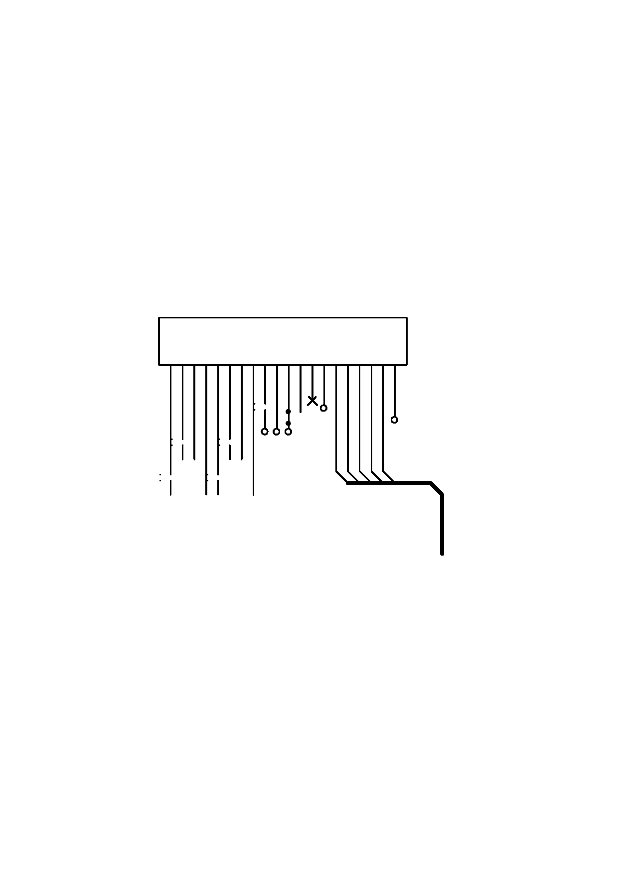
1.4 Terminal Functions(FPC)
Descriptions
Pin No. Pin Name
I/O
3-Wire SPI-S9
( Dafault )
4-Wire SPI(S8)
2-Wire SPI(IIC)
1
VB0+
Power DC-DC Booster capacitors
2
VB1+
Control data or Display data Selection for read/write operation.
3
VB1-
In S9 and I2C mode,CD pin is not used,connect CD pin to Vss.
4
VB0-
“L”:Control data
“H”:Display data
5
VA0+
6
VA1+
7
VA1-
8
VA0-
9
VLCD
Power LCD power supply
10
VDD
Power Positive Power Supply
11
VSS
Power 0V Supply, Ground (0V)
12
VSS
Power 0V Supply, Ground (0V)
13
TST4
Input Normal leave open
14
BM0
Input
H
L
H
15
CD
Input Not used,
Control data or Display data
Not used,
please connect
selection for ‘Read” or “Write”
please connect to
to VSS.
operation.
VSS.
“L”:Control data
“H”:Display data
16
A3(CS1)
Input Chip Select
Use to configure
CS1=H, enable access to the LCD module
the address of the
CS1=L, disable access to the LCD module
device
17
/RST
Input Rest input pin,when /RST is”L”,initialization is excuted
18
SCK
Input Serial clock input
19
SDA
Input Serial data input
20
I 2 C/SPI
Input
L
L
H
1.5 Blacklight Terminal
Pin No. Pin Name
I/O
Descriptions
Wire color
1
BLA
Power Blacklight positive power supply
Red
2
BLK
Power Blacklight negative power supply
white
URL: www.topwaydisplay.com
Document Name: LM24064JFW-Manual-Rev.0.4
www.topwaysz.com
Page: 4 of 17
TOPWAY
LCD Module User Manual
LM24064JFW
2. Absolute Maximum Ratings
Items
Symbol
Min.
Max.
Unit
Condition
Supply Voltage
V DD
-0.3
+4.0
V
V SS = 0V
Input Voltage
V IN
-0.3
V DD +0.3
V
V SS = 0V
Operating Temperature
T OP
-20
+70
C
No Condensation
Storage Temperature
T ST
-30
+80
C
No Condensation
Mean Time Between Failure
MTBF
100000
-
HRS
No Condensation
Cautions:
Any Stresses exceeding the Absolute Maximum Ratings may cause substantial damage to the device. Functional
operation of this device at other conditions beyond those listed in the specification is not implied and prolonged exposure
to extreme conditions may affect device reliability.
3. Electrical Characteristics
3.1 DC Characteristics
V SS =0V, V DD =3.3V, T OP =25 C
Items
Symbol
MIN.
TYP
MAX.
Unit Condition /
.
Application Pin
Operating Voltage
V DD
3.0
3.3
3.6
V
VDD
Input High Voltage
V IH
0.8xV DD
-
V DD
V
SDA,SCK,/RST,CS1,CD
Input Low Voltage
V IL
0
-
0.2xV DD
V
Operating Current
I DD
-
0.63
1.6
mA VDD
3.2 LED Backlight Circuit Characteristics
V SS =0V, If BLA =136mA,T OP =25 C
Items
Symbol
MIN.
TYP.
MAX.
Unit
Applicable Pin
Forward Voltage
Vf BLA
-
3.3
-
V
BLA
Forward Current
If BLA
-
136
160
mA
BLA
Life Time
-
-
50000
-
HRS
Cautions:
Exceeding the recommended driving current could cause substantial damage to the backlight and shorten its lifetime.
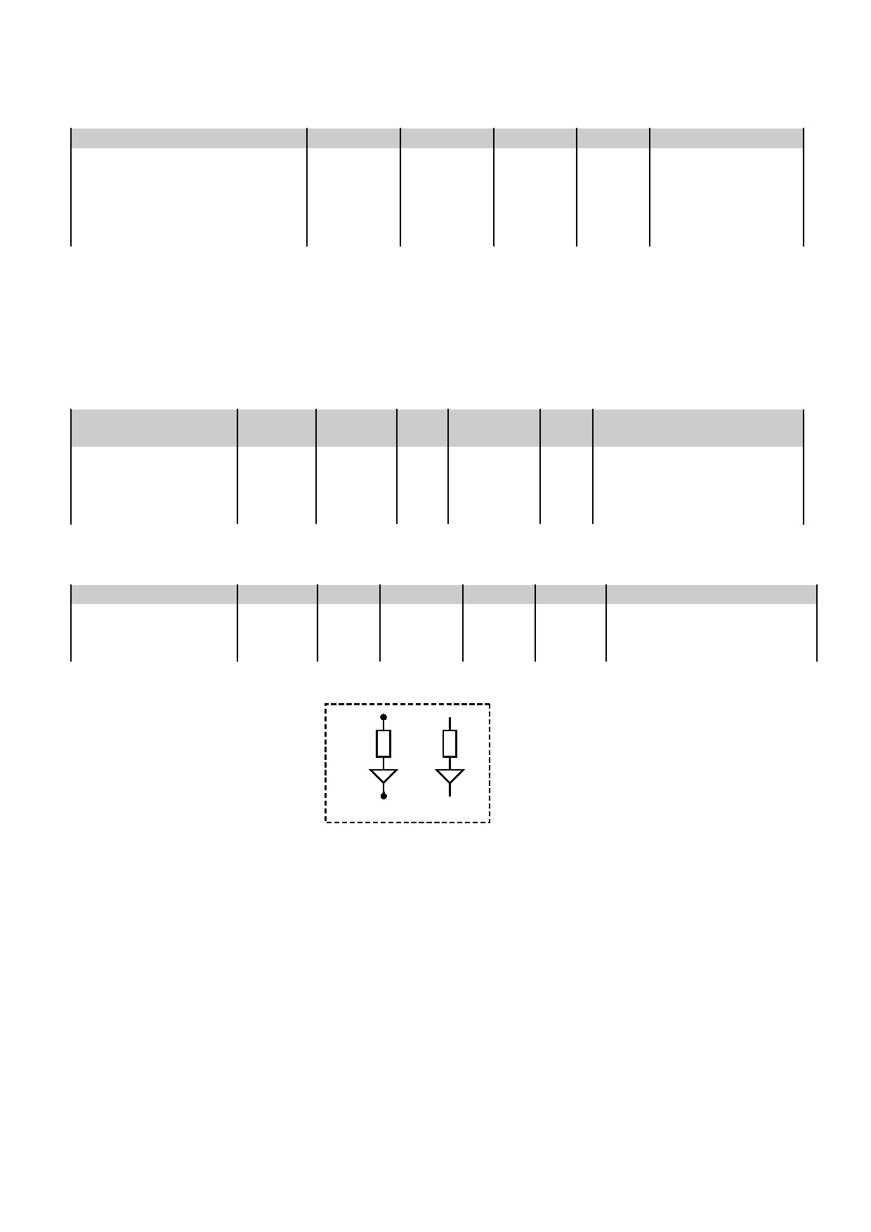
BLA
…
BLK
No. of LED = 8PCS
URL: www.topwaydisplay.com
Document Name: LM24064JFW-Manual-Rev.0.4
www.topwaysz.com
Page: 5 of 17
TOPWAY
LCD Module User Manual
LM24064JFW
3.3 AC Characteristics
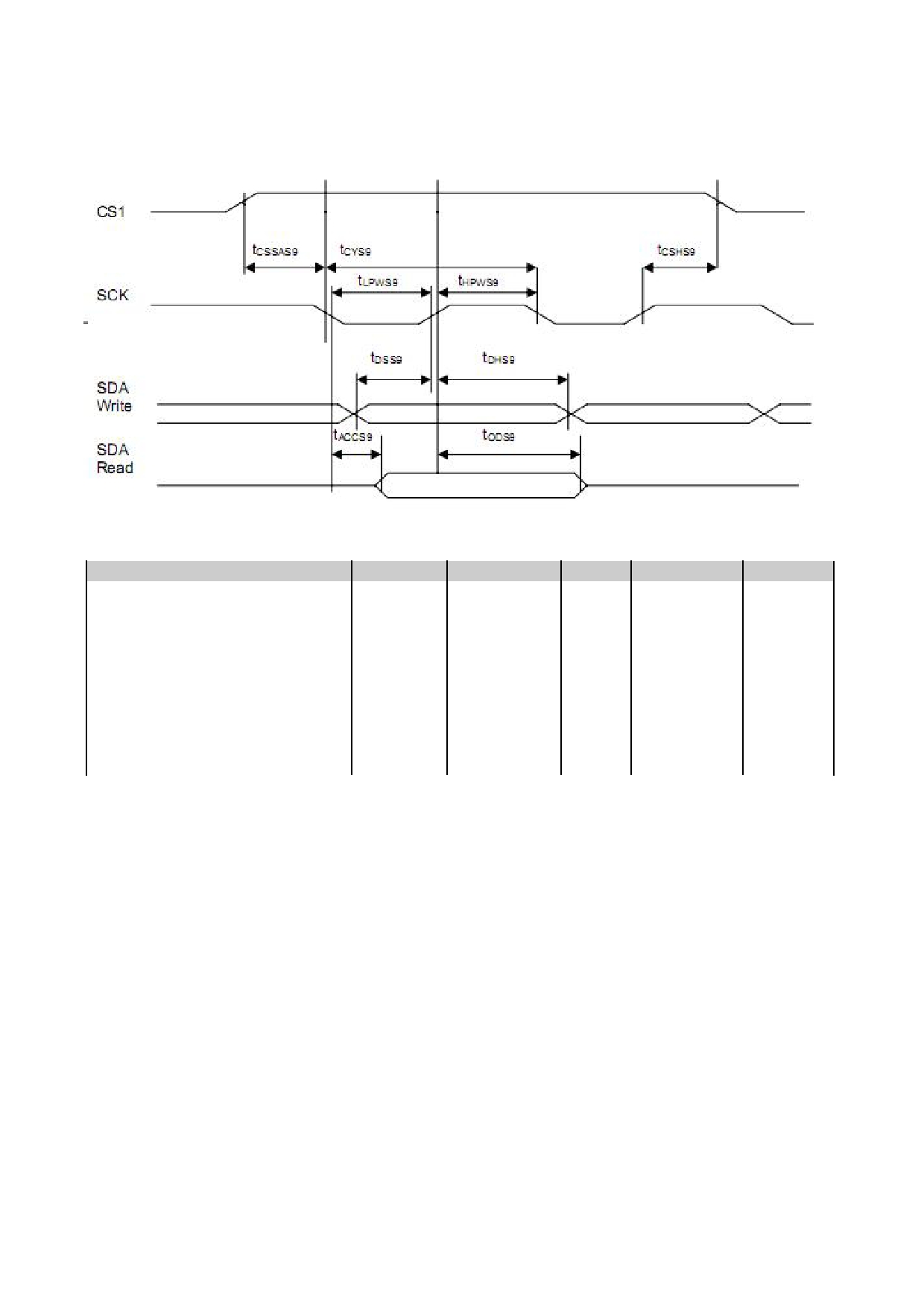
3.3.1 3-Wire Serial Interface(Default)
V SS =0V, V DD =3.3V, T OP =25 C
Item
Symbol
MIN.
TYP.
MAX.
Unit
System cycle tim ( Read/Write )
t CYS9
156/46
-
-
ns
Low pulse width ( Read/Write )
T LPWS9
78/23
-
-
ns
High pulse width ( Read/Write )
T HPWS9
78/23
-
-
ns
Read access time
T ACCS9
-
-
35
ns
Output disable time(Read)
T 0DS9
20
-
-
ns
Data setup time(Write)
T DSS9
20
-
-
ns
Data hold time ( Write )
T DHS9
0
-
-
ns
Chip select setup time
T CSSAS9
0
-
-
ns
T CSHS9
0
-
-
ns
URL: www.topwaydisplay.com
Document Name: LM24064JFW-Manual-Rev.0.4
www.topwaysz.com
Page: 6 of 17
TOPWAY
LCD Module User Manual
LM24064JFW
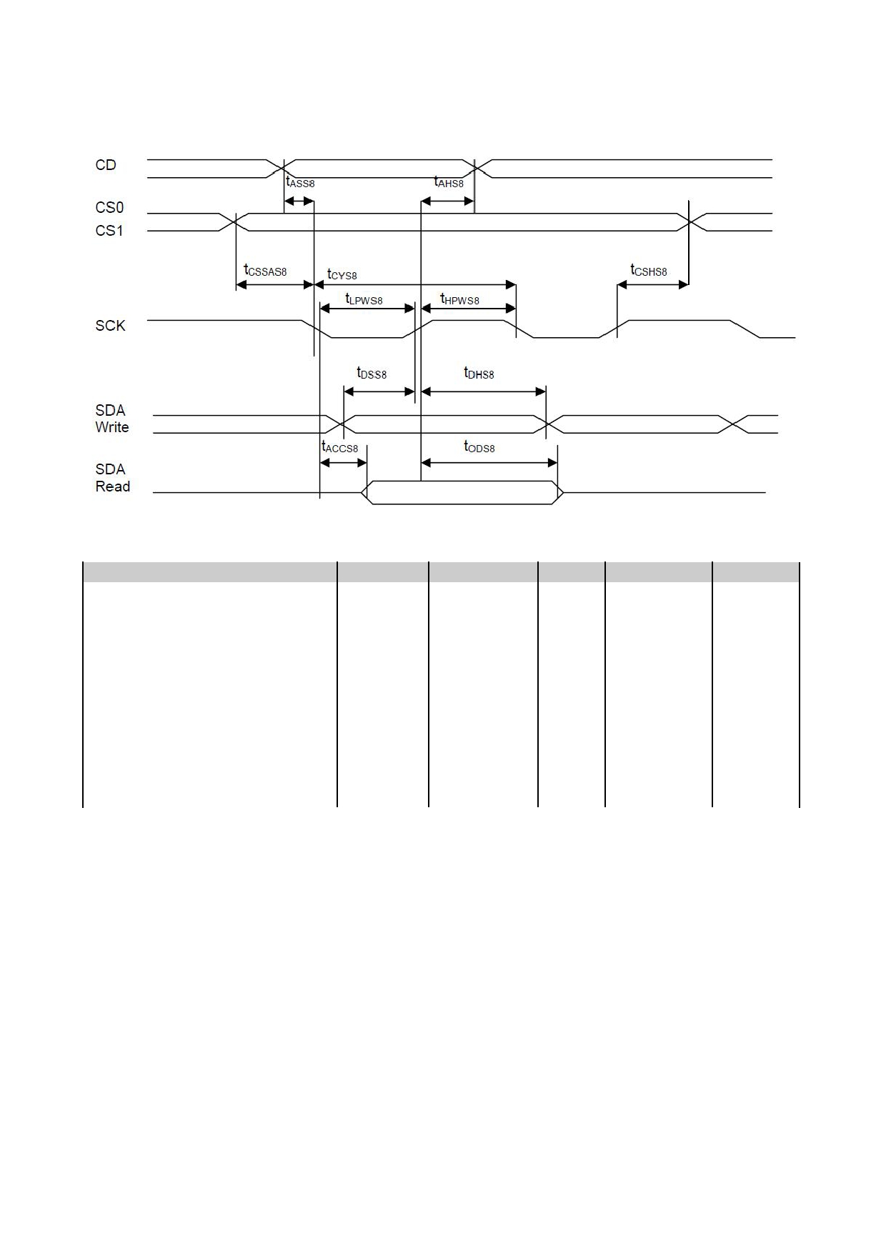
3.3.2 4-Wire Serial Interface
V SS =0V, V DD =3.3V, T OP =25 C
Item
Symbol
MIN.
TYP.
MAX.
Unit
Address setup time
t ASS8
0
Address hold time
t AHS8
0
System cycle tim ( Read/Write )
t CYS8
156/46
-
-
ns
Low pulse width ( Read/Write )
T LPWS8
78/23
-
-
ns
High pulse width ( Read/Write )
T HPWS8
78/23
-
-
ns
Read access time
T ACCS8
-
-
35
ns
Output disable time(Read)
T 0DS8
20
-
-
ns
Data setup time(Write)
T DSS8
20
-
-
ns
Data hold time ( Write )
T DHS8
0
-
-
ns
Chip select setup time
T CSSAS8
0
-
-
ns
T CSHS8
0
-
-
ns
URL: www.topwaydisplay.com
Document Name: LM24064JFW-Manual-Rev.0.4
www.topwaysz.com
Page: 7 of 17
TOPWAY
LCD Module User Manual
LM24064JFW
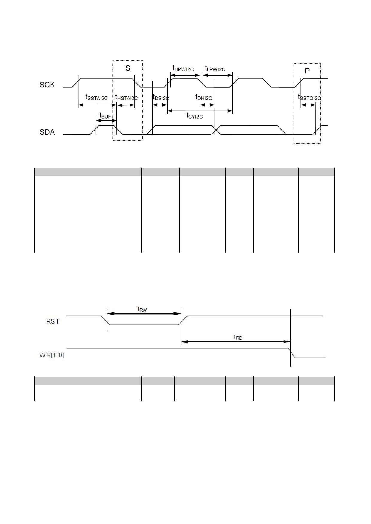
3.3.3 I 2 C mode Interface
V SS =0V, V DD =3.3V, T OP =25 C
Item
Symbol
MIN.
TYP.
MAX.
Unit
SCK cycle time ( Read/Write )
t CYI2C
754/360
-
-
ns
Low pulse width ( Read/Write )
t LPWI2C
377/180
-
-
ns
High pulse width ( Read/Write )
t HPWI2C
377/180
-
-
ns
Data setup time
t DSI2C
43
-
-
ns
Data hold time
t DHI2C
15
-
-
ns
START Setup time
t SSTAI2C
36
-
-
ns
START Hold time
t HSTAI2C
65
-
-
ns
STOP setup time
t SSTOI2C
36
-
-
ns
Bus Free time
t BUF
215
-
-
ns
Note:
*1. Input signal rise/fall time should be less than 70ns
*2 Other kind of serial mode,please refer to the datasheet of UC1611S
3.4 Reset Timing
V SS =0V, V DD =3.3V, T OP =25 C
Item
Symbol
MIN.
TYP.
MAX.
Unit
Reset low pulse width
t RW
4
-
-
us
Reset to WR pulse delay
t RD
13
-
-
ms
URL: www.topwaydisplay.com
Document Name: LM24064JFW-Manual-Rev.0.4
www.topwaysz.com
Page: 8 of 17
TOPWAY
LCD Module User Manual
LM24064JFW
4. Optical Characteristics
4.1 Optical Characteristics
T OP =25 C
Item
Symbol
MIN.
TYP.
MAX. Unit note
Viewing Direction
Φ
-
6H
-
-
Vop=typ.
On Time
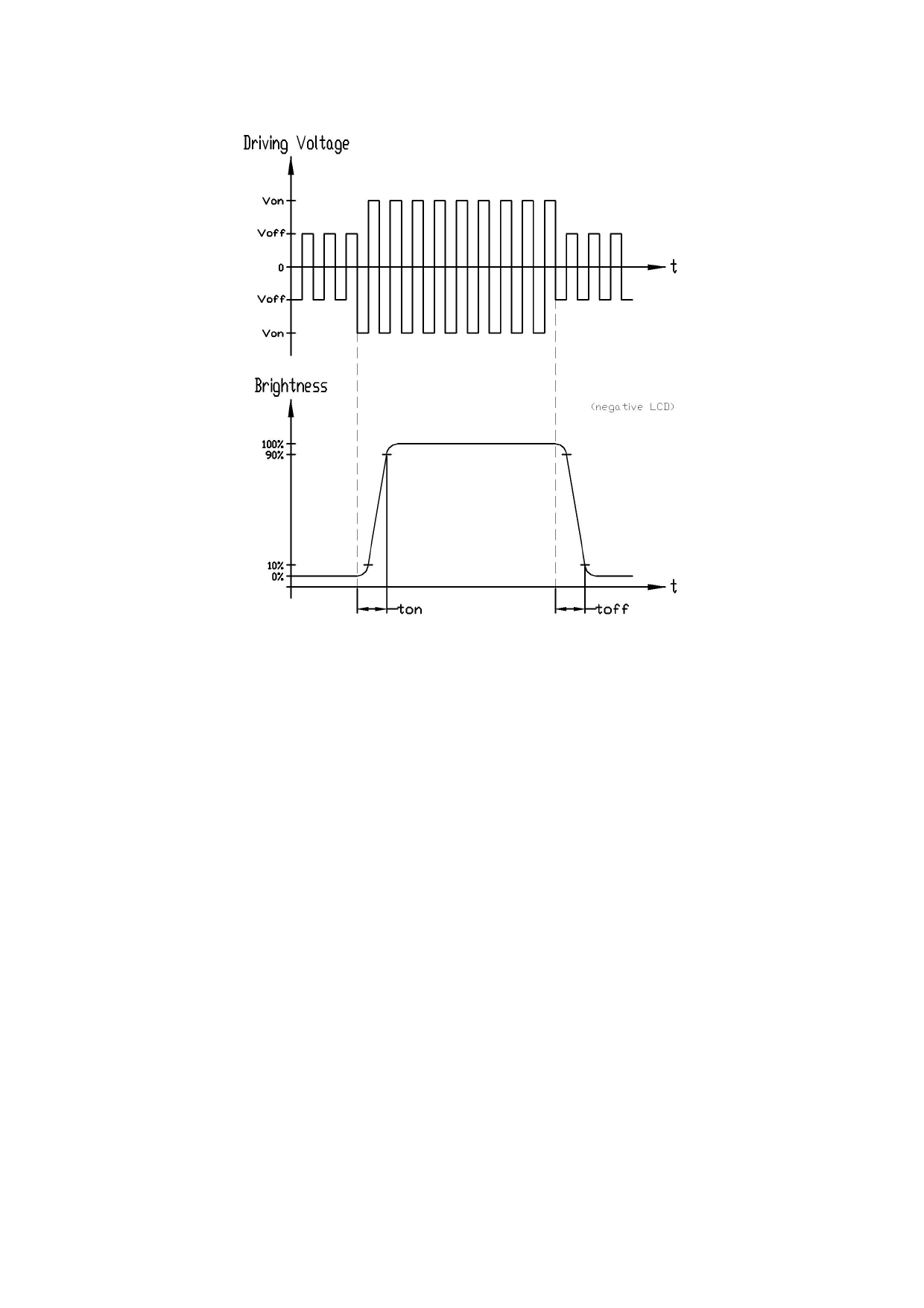
ton
-
82
-
ms X, Y = 0 , Vop=typ.
Off Time
toff
-
135
-
ms X, Y = 0 , Vop=typ.
LCD Operating Voltage
Vop
-
13
-
V
X, Y = 0
3H
-
37
-
deg
View Angle
9H
-
36
-
deg
Contrast>40%MCR *1
6H
-
45
-
deg
12H
-
38
-
deg
Contrast ratio
Cr
--
3
--
Contrast ratio
Note:
*1 MCR=Display Maximum Contrast Ratio
4.2 Definition
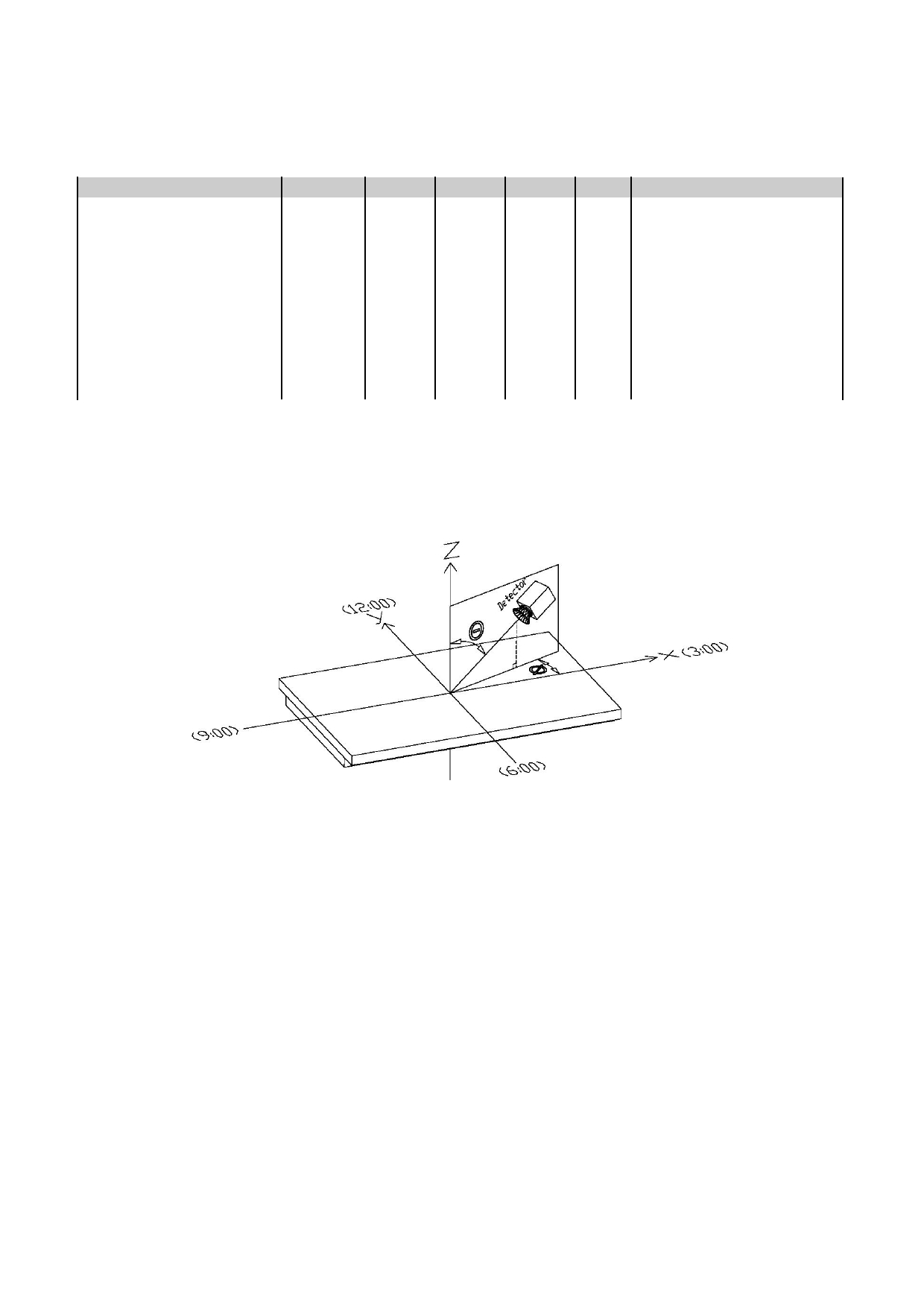
4.2.1 Viewing Direction
Viewing Direction = direction (Φ) that provide the best display result
URL: www.topwaydisplay.com
Document Name: LM24064JFW-Manual-Rev.0.4
www.topwaysz.com
Page: 9 of 17
TOPWAY
LCD Module User Manual
LM24064JFW
4.2.2 Response Time
URL: www.topwaydisplay.com
Document Name: LM24064JFW-Manual-Rev.0.4
www.topwaysz.com
Page: 10 of 17
TOPWAY
LCD Module User Manual
LM24064JFW
5. Function Specifications
5.1 Adjusting the Display Contrast
- This LCD module equipped with latest digital contrast adjustment function.
- Its display contrast could be adjusted by MCU command. (please see the command tables for
details)
It is recommended to provide a contrast adjustment interface for end-user, where the best display
result could meet the individual preference in mass production.
5.2 Resetting the LCD module
The LCD module should be initialized by using /RST terminal.
While turning on the VDD and VSS power supply, maintain /RST terminal at LOW level. After the
power supply stabilized, release the reset terminal (/RST=HIGH)
5.3 Application circuit (Example)
LCM
LM24064J
C1
C2
C3
C4
C5
1.0uF 1.0uF 1.0uF 1.0uF 1.0uF
16V 16V 16V 16V 25V
NOTE:
*1. Using internal step up booster
*2. 3 wire serial mode
URL: www.topwaydisplay.com
Document Name: LM24064JFW-Manual-Rev.0.4
www.topwaysz.com
Page: 11 of 17

TOPWAY
LCD Module User Manual
LM24064JFW
5.4 Display Memory Map
Page data
LCD Display (front view)
D0
0
:
D7
D0
1
:
D7
D0
2
:
D7
:
:
:
240x64 Pixels
:
D0
5
:
D7
D0
6
:
D7
D0
7
:
D7
Column
Address
……
(dec)
Pixel mapping (Top View)
Note:
* 1. Based on the top view of the LCD module,
*2. The above is memory map based on:
On/Off mode setting, DC[5:3]=100 (1bpp) ,the Page value range: 0 ~ 7
LC[0]=MSF=0
LC[1]=MX=1
LC[2]=MY=0
SL=0
*3. For 4,8 and 16 Gray-shade operation please refer to UC1611S datasheet.
URL: www.topwaydisplay.com
Document Name: LM24064JFW-Manual-Rev.0.4
www.topwaysz.com
Page: 12 of 17
TOPWAY
LCD Module User Manual
LM24064JFW
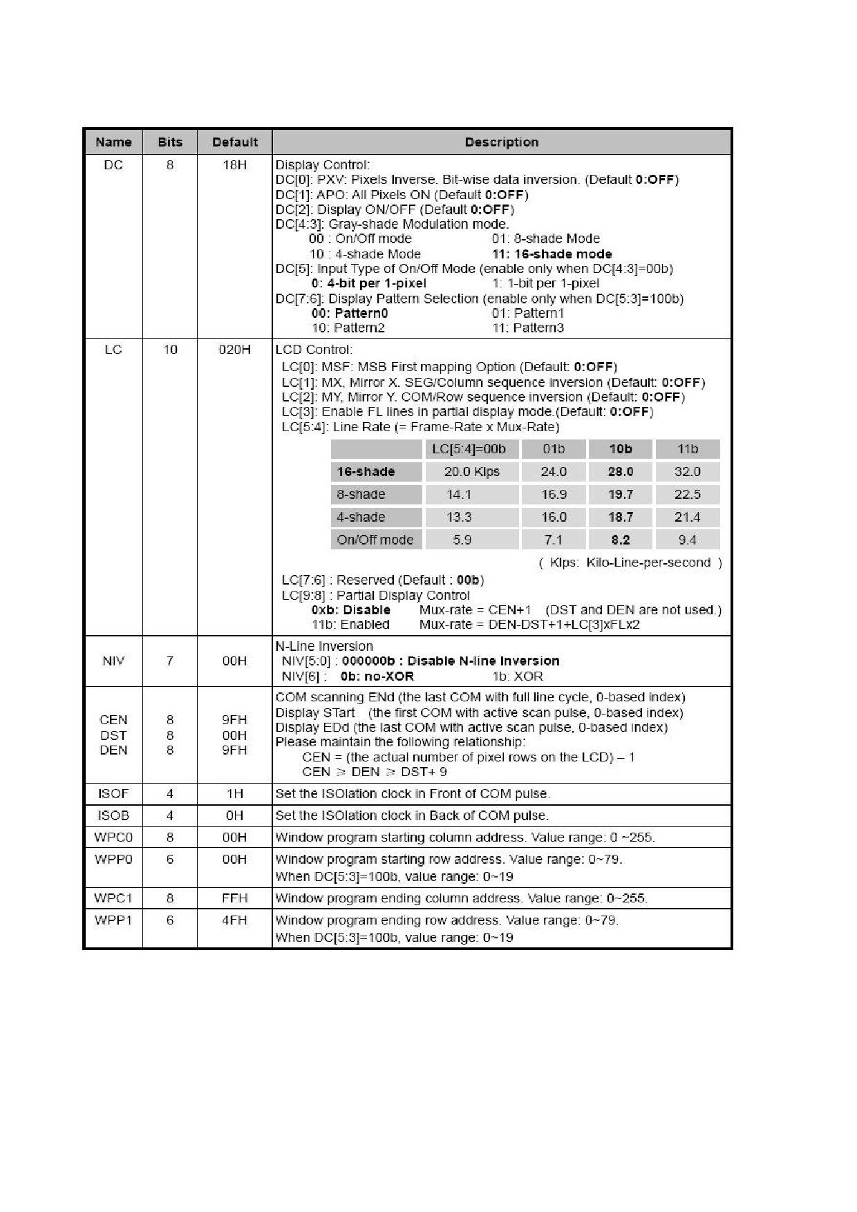
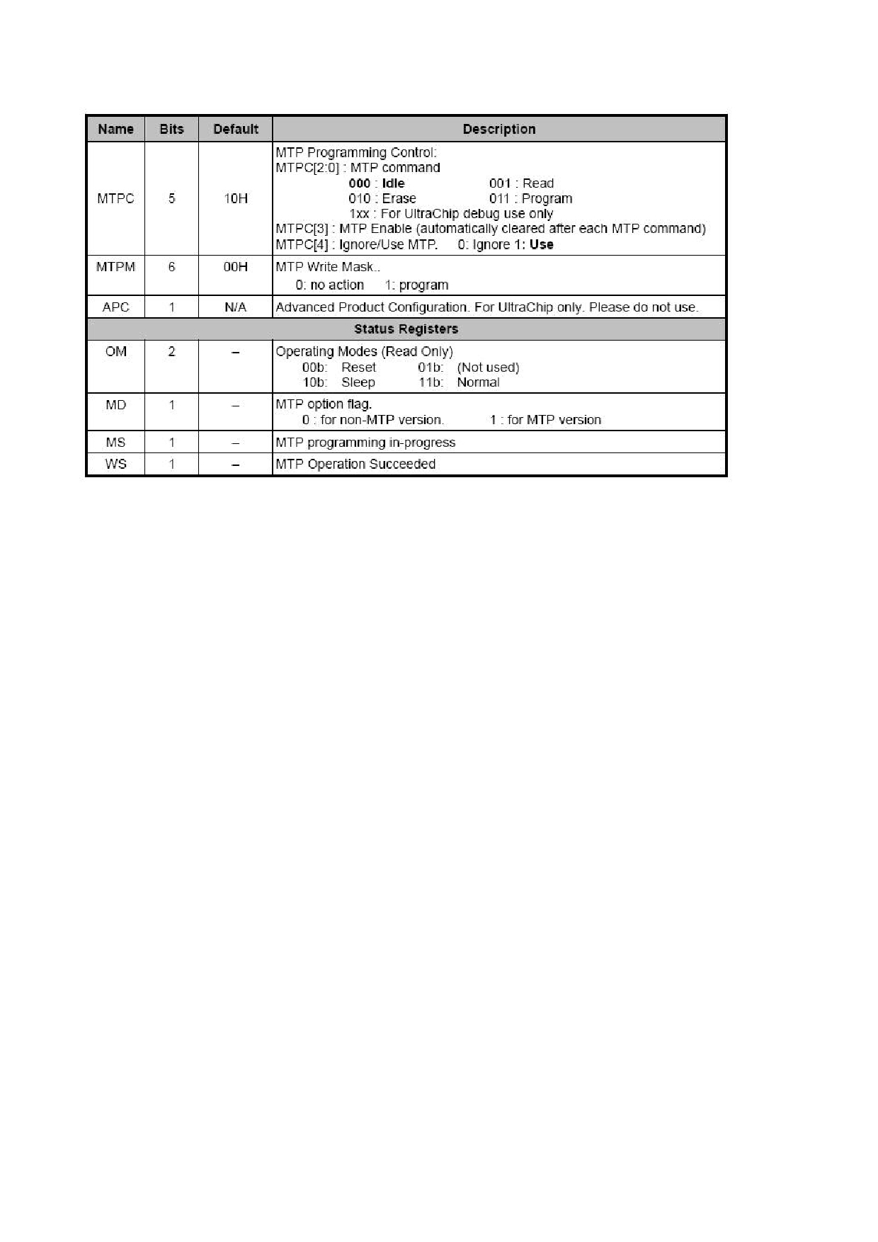
5.5 Commands
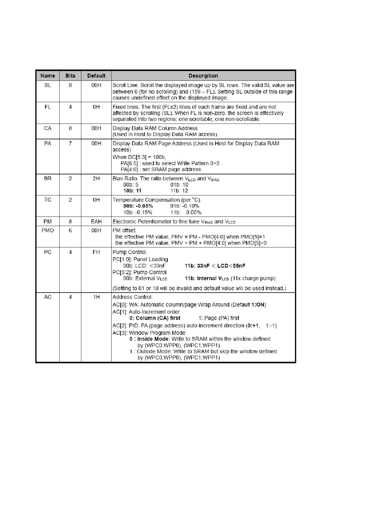
5.5.1 Register Table
URL: www.topwaydisplay.com
Document Name: LM24064JFW-Manual-Rev.0.4
www.topwaysz.com
Page: 13 of 17
TOPWAY
LCD Module User Manual
LM24064JFW
Register Table (continue)
URL: www.topwaydisplay.com
Document Name: LM24064JFW-Manual-Rev.0.4
www.topwaysz.com
Page: 14 of 17
TOPWAY
LCD Module User Manual
LM24064JFW
Register Table (continue)
URL: www.topwaydisplay.com
Document Name: LM24064JFW-Manual-Rev.0.4
www.topwaysz.com
Page: 15 of 17
TOPWAY
LCD Module User Manual
LM24064JFW
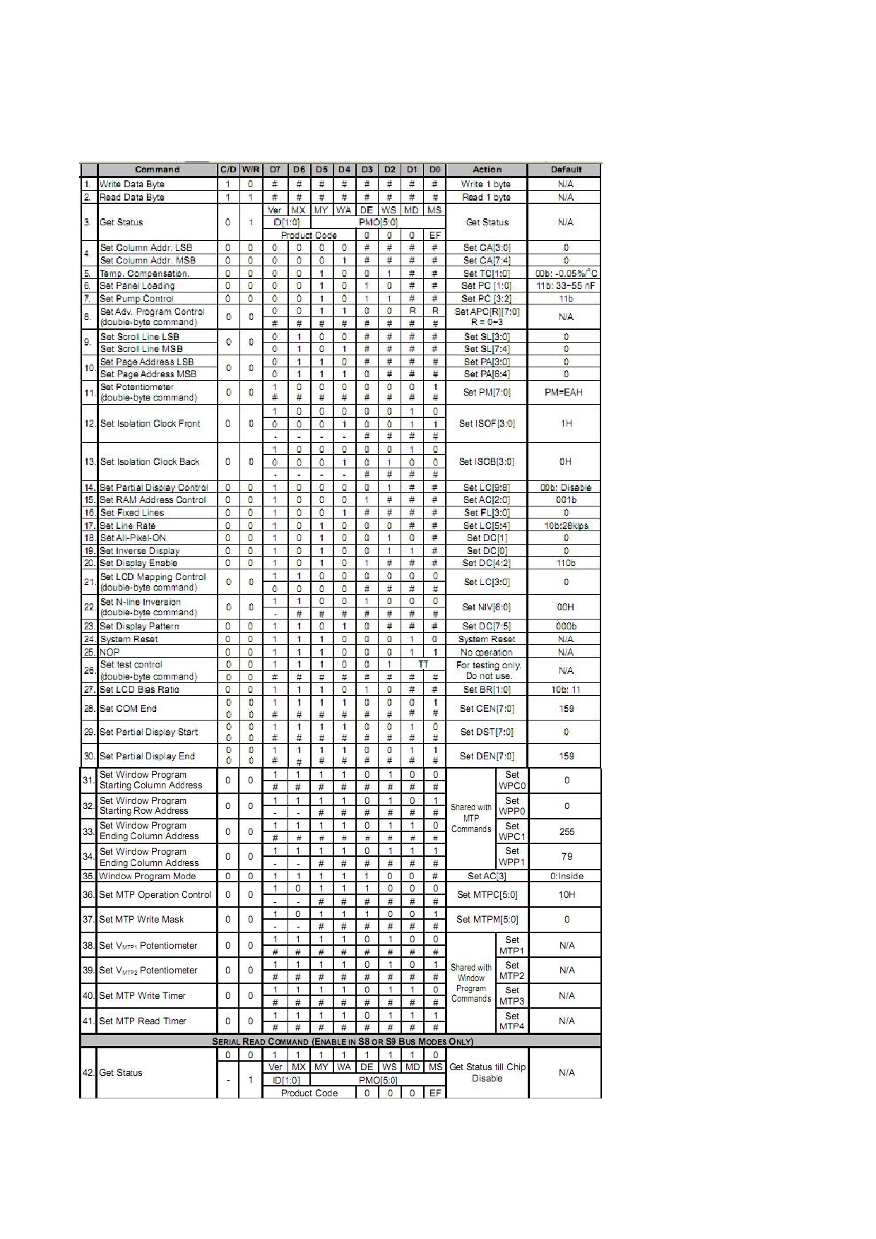
5.6 Command Table
The following setting should be issue to LCD module after hardware reset.
(It is an example only; it could be adjusted if necessary.)
Note:
Please refer to UC1611S data sheet for details
R/W=0 means it is a write function, R/W=1 means it is a read function
C/D=0 means it is a control data, C/D=1 means it is a display data
URL: www.topwaydisplay.com
Document Name: LM24064JFW-Manual-Rev.0.4
www.topwaysz.com
Page: 16 of 17

TOPWAY
LCD Module User Manual
LM24064JFW
6. Design and Handling Precaution
1.
The LCD panel is made by glass. Any mechanical shock (eg. dropping form high place)
will damage the LCD module.
2.
Do not add excessive force on the surface of the display, which may cause the Display
color change abnormally.
3.
The polarizer on the LCD is easily get scratched. If possible, do not remove the LCD
protective film until the last step of installation.
4.
Never attempt to disassemble or rework the LCD module.
5.
Only Clean the LCD with Isopropyl Alcohol or Ethyl Alcohol. Other solvents (eg. water)
may damage the LCD.
6.
When mounting the LCD module, make sure that it is free form twisting, warping and
distortion.
7.
Ensure to provide enough space (with cushion) between case and LCD panel to prevent
external force adding on it, or it may cause damage to the LCD or degrade the display
result.
8.
Only hold the LCD module by its side. Never hold LCD module by add force on the heat
seal or TAB.
9.
Never add force to component of the LCD module. It may cause invisible damage or
degrade of the reliability.
10.
LCD module could be easily damaged by static electricity. Be careful to maintain an
optimum anti-static work environment to protect the LCD module.
11.
When peeling off the protective film from LCD, static charge may cause abnormal
display pattern. It is normal and will resume to normal in a short while.
12.
Take care and prevent get hurt by the LCD panel sharp edge.
13.
Never operate the LCD module exceed the absolute maximum ratings.
14.
Keep the signal line as short as possible to prevent noisy signal applying to LCD module.
15.
Never apply signal to the LCD module without power supply.
16.
IC chip (eg. TAB or COG) is sensitive to the light. Strong lighting environment could
possibly cause malfunction. Light sealing structure casing is recommend.
17.
LCD module reliability may be reduced by temperature shock.
18.
When storing the LCD module, avoid exposure to the direct sunlight, high humidity, high
temperature or low temperature. They may damage or degrade the LCD module
Document Name: LM24064JFW-Manual-Rev.0.4
Page: 17 of 17