LM6060CFW-3
LCD Module User Manual
Prepared by:
Checked by:
Approved by:
liangquan
Date: 2015-11-19
Date:
Date:
Rev. Descriptions
Release Date
0.1
Preliminary release
2015-11-19
URL: www.topwaydisplay.com
Document Name: LM6060CFW-3-Manual-Rev0.1
Page: 1 of 12

TOPWAY
LCD Module User Manual
LM6060CFW-3
Table of Content
1. Basic Specifications .............................................................................................................. 3
1.1
Display Specifications ............................................................................................................................................ 3
1.2
Mechanical Specifications ...................................................................................................................................... 3
1.3
Block Diagram ........................................................................................................................................................ 3
1.4
Terminal Functions ................................................................................................................................................. 4
Absolute Maximum Ratings ......................................................................................................... 4
2. Electrical Characteristics ...................................................................................................... 5
2.1
DC Characteristics ................................................................................................................................................. 5
2.2
LED Backlight Circuit Characteristics ..................................................................................................................... 5
2.3
AC Characteristics ................................................................................................................................................. 6
2.4
Reset Timing .......................................................................................................................................................... 7
3. Function specifications ......................................................................................................... 7
3.1
Adjusting the Display Contrast ............................................................................................................................... 7
3.2
The Serial Interface ................................................................................................................................................ 7
3.3
Basic Setting .......................................................................................................................................................... 8
3.4
Resetting the LCD module ..................................................................................................................................... 8
3.5
Display Memory Map.............................................................................................................................................. 8
3.6
Display Commands ................................................................................................................................................ 9
3.7
Display Commands (continue) ............................................................................................................................. 10
3.8
Basic Operating Sequence (example) .................................................................................................................. 11
4. Design and Handling Precaution ........................................................................................ 12
URL: www.topwaydisplay.com
Document Name: LM6060CFW-3-Manual-Rev0.1
Page: 2 of 12
TOPWAY
LCD Module User Manual
LM6060CFW-3
1. Basic Specifications
1.1 Display Specifications
1) LCD Display Mode
: STN-Blue, Negative, Transmissive
2) Display Color
: Display Data = “1” : Lighe Gray(*1)
: Display Data = “0” : Deep Blue (*2)
3) Viewing Angle
: 6H
4) Driving Method
: 1/65 duty, 1/9 bias
5) Backlight
: White LED backlight
Note:
*1. Color tone may slightly change by Temperature and Driving Condition.
*2. The Color is defined as the inactive / background color
*3. Fine Contrast adjustment function is necessary in the application design for optimal display result
1.2 Mechanical Specifications
1) Outline Dimension
: 73.0 x 42.0 x 10.9MAX (mm)(Exclude FFC)
(See attached Outline Drawing for details)
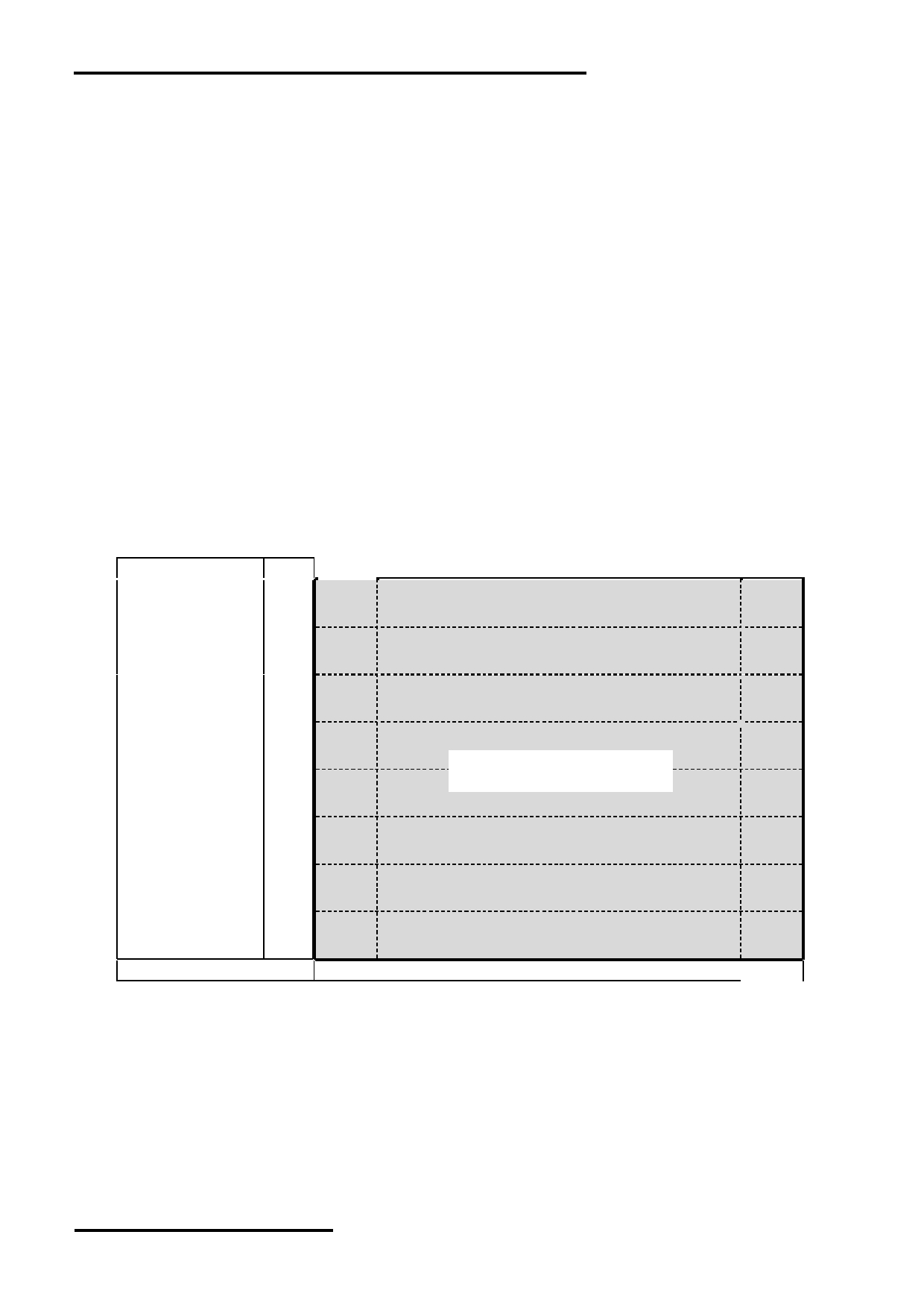
1.3 Block Diagram
BLA
Backlight Circuit
LCD Panel
128 × 64Pixels
VDD
VSS
ST7565 or equivalent
SCL,SI
/CS1, /RES, A0
URL: www.topwaydisplay.com
Document Name: LM6060CFW-3-Manual-Rev0.1
Page: 3 of 12
TOPWAY
LCD Module User Manual
LM6060CFW-3
1.4 Terminal Functions
PIN NO
PIN Name
I/O
Descriptions
1
BLA
Supply Positive power for LED backlight
2
/CS1
Input
Chip Select
/CS1=L, enable access to the LCD module
/CS1=H, disable access to the LCD module
3
/RES
Input
Reset signal
/RES = L, Initialization is executed
/RES = H, Normal running.
4
A0
Input
Register Select
A0 = H, Transferring the Display Data
A0 = L, Transferring the Control Data
5
SCL
I/O
Serial clock input
6
SI
I/O
Serial data input
7
VSS
Supply Negative power supply,0V
8
VDD
Supply Positive power supply
Absolute Maximum Ratings
Items
Symbol
Min.
Max.
Unit Condition
Supply Voltage
V DD
-0.3
+3.3
V
V SS = 0V
Input Voltage
V IN
-0.3
V DD +0.3
V
V SS = 0V
Operating Temperature
T OP
-20
+70
C
No Condensation
Storage Temperature
T ST
-30
+80
C
No Condensation
Cautions:
Any Stresses exceeding the Absolute Maximum Ratings may cause substantial damage to the device. Functional
operation of this device at other conditions beyond those listed in the specification is not implied and prolonged exposure
to extreme conditions may affect device reliability.
URL: www.topwaydisplay.com
Document Name: LM6060CFW-3-Manual-Rev0.1
Page: 4 of 12

TOPWAY
LCD Module User Manual
LM6060CFW-3
2. Electrical Characteristics
2.1 DC Characteristics
V SS =0V, V DD =3.3V, T OP =25 C
Items
Symbol
MIN.
TYP.
MAX.
Unit Condition /
Application Pin
Operating Voltage
V DD
2.8
-
3.3
V
VDD
Input High Voltage
V IH
0.8xV DD
-
V DD
V
/RES, /CS1, A0,
Input Low Voltage
V IL
V SS
-
0.2xV DD
V
SCL,SI
Operating Current
I DD
-
0.3
1.5
mA VDD
2.2 LED Backlight Circuit Characteristics
BLK=0V, BLA=3.3V, T OP =25 C
Items
Symbol
MIN.
TYP.
MAX.
Unit Applicable Pin
Forward Voltage
BLA
-
3.3
-
V
BLA
Forward Current
I BLA
-
48
50
mA BLA
BLA
………..
BLK
No. of LED = 3 pcs
URL: www.topwaydisplay.com
Document Name: LM6060CFW-3-Manual-Rev0.1
Page: 5 of 12
TOPWAY
LCD Module User Manual
LM6060CFW-3
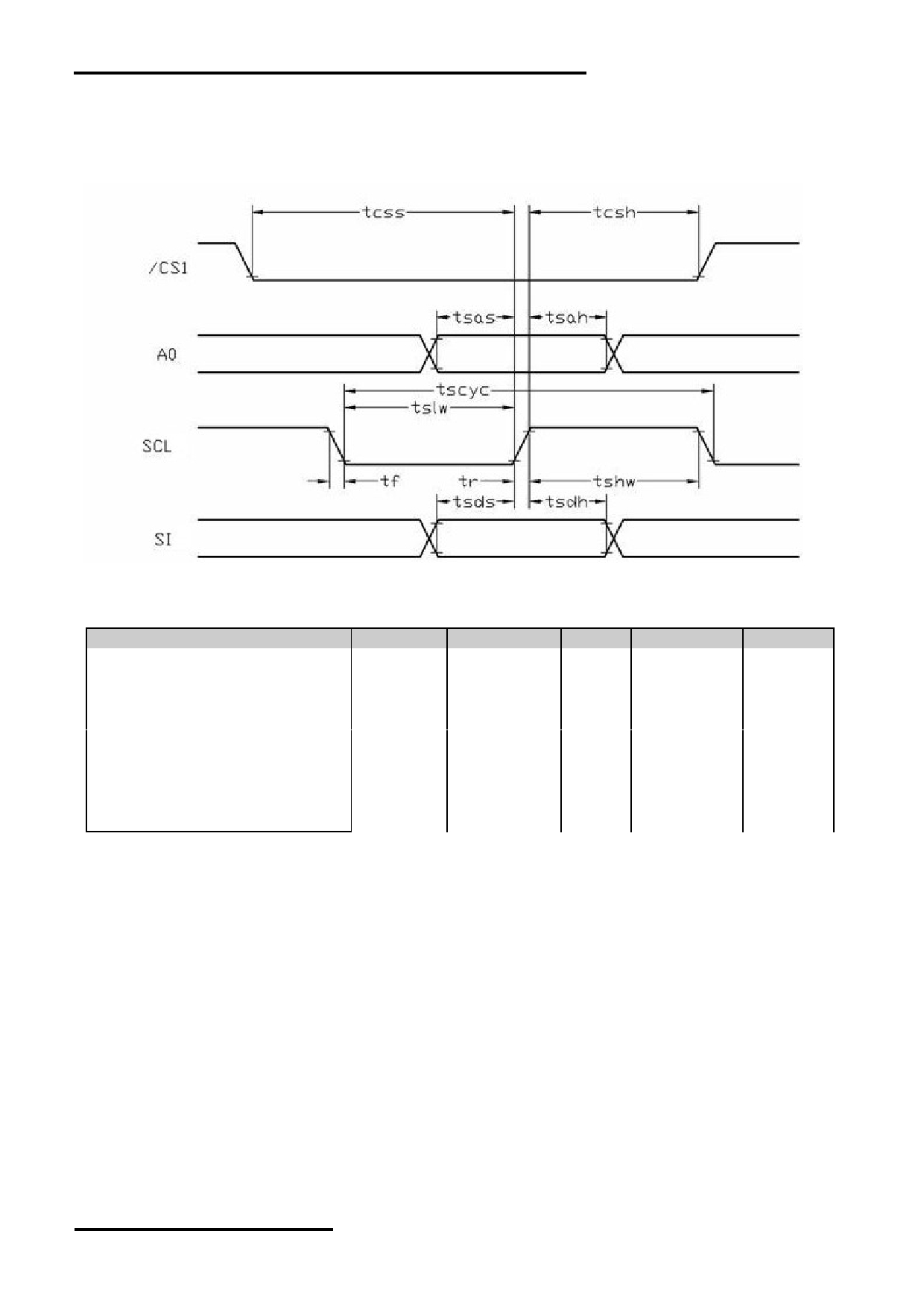
2.3 AC Characteristics
2.3.1 Serial Mode Interface
V SS =0V, V DD =3.0V, T OP =25 C
Item
Symbol
MIN.
TYP.
MAX.
Unit
Serial Clock Period
tscyc
125
-
-
ns
Address setup time (A0)
tsas
38
-
-
ns
Address hold time (A0)
tsah
25
-
-
ns
SCL “H” pulse width
tshw
63
-
-
ns
SCL “L” pulse width
tslw
63
-
-
ns
Data setup time
tsds
38
-
-
ns
Data hold time
tsdh
25
-
-
ns
/CS1-SCL time
tcss
38
-
-
ns
/CS1-SCL time
tcsh
75
-
-
ns
Note:
*1. Input signal rise/fall time should be less than 15ns .
*2. CL=100pF
*3.All timing is using 20% and 80% of VDD as the reference.
URL: www.topwaydisplay.com
Document Name: LM6060CFW-3-Manual-Rev0.1
Page: 6 of 12

TOPWAY
LCD Module User Manual
LM6060CFW-3
2.4 Reset Timing
V SS =0V, V DD =3.0V, T OP =25 C
Item
Symbol
MIN.
TYP.
MAX.
Unit
Reset time
tr
-
-
2.5
μs
Reset LOW pulse width
trw
2.5
-
-
μs
Note:
*1.All timing is using 20% and 80% of VDD as the reference.
3. Function specifications
3.1 Adjusting the Display Contrast
- This LCD module equipped with latest digital contrast adjustment function.
- Its display contrast could be adjusted by MCU command. (please see the command tables for
details)
- It is recommended to provide a contrast adjustment interface for end-user, where the best
display result could meet the individual preference in mass production.
3.2 The Serial Interface
When the serial interface has been selected then when the chip is in active state the serial data
input(SI) and the serial clock(SCL) can be received. The serial data is read from the serial data
input pin in the rising edge of the serial clock . When “A0”=“H”, the data is display data, and when
“A0”=“L”, the data is command.
URL: www.topwaydisplay.com
Document Name: LM6060CFW-3-Manual-Rev0.1
Page: 7 of 12
TOPWAY
LCD Module User Manual
LM6060CFW-3
3.3 Basic Setting
To drive the LCD module correctly and provide normally display, please use the following setting
- ADC = 0 (normal)
- SHL select = 1 (reverse)
- LCD Bias Select = 1/9
- Initial Display Line = 0
- Entire Display ON/OFF = OFF (normal)
- Reverse Display ON/OFF = OFF (normal)
- Set Power Control Set:
voltage follower = ON, voltage converter = ON, voltage regulator = ON
- Booster Set = 4x
- Display ON/OFF = ON
Note:
*1. These setting/commands should issue the LCD module while start up.
*2. See the Display Commands section for details.
3.4 Resetting the LCD module
The LCD module should be initialized by using /RES terminal.
While turning on the VDD and VSS power supply, maintain /RES terminal at LOW level. After the
power supply stabilized, release the reset terminal (/RES=HIGH)
3.5 Display Memory Map
Page address
data
LCD Display (front view)
D0
0
:
D7
D0
1
:
D7
D0
2
:
D7
D0
3
:
D7
D0
4
:
128x64 pixels
D7
D0
5
:
D7
D0
6
:
D7
D0
7
:
D7
Column Address
00h
7Fh
Note:
*1. ADC = 0 (normal)
*2. SHL Selection = 1 (reverse)
*3. Initial Display Line = 0
URL: www.topwaydisplay.com
Document Name: LM6060CFW-3-Manual-Rev0.1
Page: 8 of 12

TOPWAY
LCD Module User Manual
LM6060CFW-3
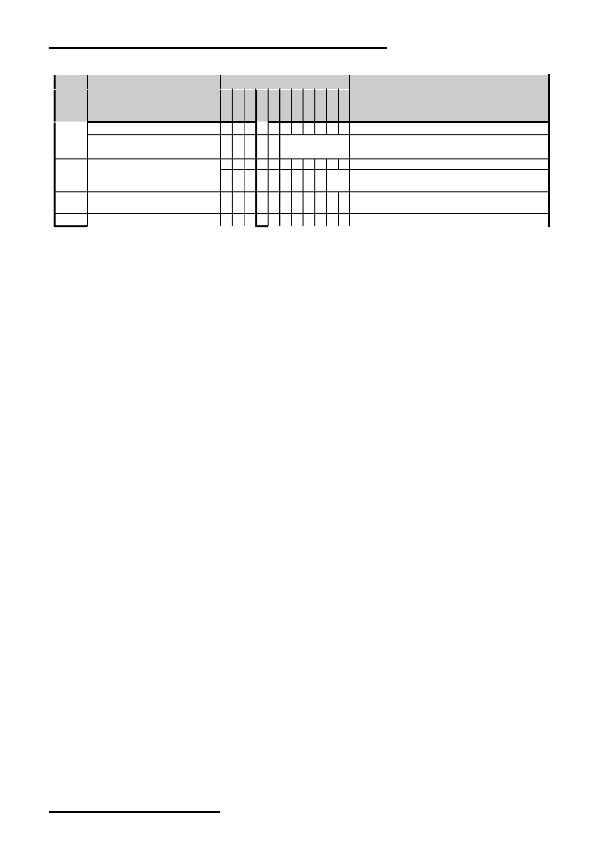
3.6 Display Commands
Code
No. Instructions
Function
DON=0, display off
1
Display ON/OFF
0 1 0 1 0 1 0 1 1 1
DON=1, display oin
Display start
Sets the display RAM display start line
2
Display start line set
0 1 0 0 1
address
address
Page
3
Set Page Address
0 1 0 1 0 1 1
Address
Set the display RAM page address
Set Column Address
0 1 0 0 0 0 1
Col. Add.
Set the upper-4-bit of column address counter
(Upper-4-bits)
Upper
4
Set Column Address
0 1 0 0 0 0 0
Col. Add.
Set the lower-4-bit of column address counter
(Lower-4-bits)
Lower
Read the status data
5
Read Status
0 0 1
Status
0 0 0 0
6
Write Display Data
1 1 0
Write Data
Write data into the display RAM
7
Read Display Data
1 0 1
Read Data
Read data form the display RAM
Sets the display RAM address SEG output
8
ADC Select
0 1 0 1 0 1 0 0 0 0
correspondence
ADC= 0,normal . ADC=1, reverse
REV=0, Normal display
9
Normal/Reverse Display 0 1 0 1 0 1 0 0 1 1
REV=1, Reverse display
EON=0, Normal display
10
Entire Display ON/OFF
0 1 0 1 0 1 0 0 1 0
EON=1, Entire display ON
Set the LCD driving voltage bias
11
Set LCD Bias
0 1 0 1 0 1 0 0 0 1
BIAS=0, 1/9 BIAS
BIAS=1, 1/7 BIAS
Enter the “Read-Modify-Write” mode
column address counter will increase in each
12
Set Read-Modify-Write
0 1 0 1 1 1 0 0 0 0 0 “Write Display Data”,
and will not increase in each “Read Display
Data command”
13
Reset Read-Modify-Write 0 1 0 1 1 1 0 1 1 1 0 Clear the “Read-Modify-Write” mode
14
Reset
0 1 0 1 1 1 0 0 0 1 0 Resets the LCD module
Set the COM scanning direction
SHL=0, Normal display
15
SHL Select
0 1 0 1 1 0 0
* * *
SHL=1, Flipped in y direction
* = don’t care terms
Set the power circuit operation mode
VF: LCD Supply Voltage Follower
16
Power Control Set
0 1 0 0 0 1 0 1
VR: LCD Supply Voltage Regulator
VC: LCD Supply Voltage Converter
(1=ON, 0=OFF)
Radio
17
Regulator Resistor Select 0 1 0 0 0 1 0 0
setting
Set the built-in resistor ratio (Rb/Ra)
Note:
*1. Do not use any other command not listed, or the system malfunction may result.
*2. For the details of the Display Commands, please refer to ST7565R data sheet.
URL: www.topwaydisplay.com
Document Name: LM6060CFW-3-Manual-Rev0.1
Page: 9 of 12
TOPWAY
LCD Module User Manual
LM6060CFW-3
3.7 Display Commands (continue)
Code
No. Instructions
Function
18
Electronic volume mode set 0 1 0 1 0 0 0 0 0 0 1 Set reference voltage mode
Electronic volume register
Electronic
Set reference voltage register
set
0 1 0 * *
Control value (Display contrast value)
19
0 1 0 1 1 1 1 1 0 0 0 Select booster ratio
Booster Ratio Set
0 1 0 0 0 0 0 0 0
ste
p
00=2x,3x,4x; 01=5x. 11=6x
20
Compound Instruction:
Power Save
- - - - - - - - - - -
Display OFF + Entire Display ON
21
NOP
0 1 0 1 1 1 0 0 0 1 1 Non-operation command
Note:
*1. Do not use any other command not listed, or the system malfunction may result.
*2. For the details of the Display Commands, please refer to ST7565R data sheet.
3.7.1 Power off the LCD Module
It recommends that enter Power Save mode before power off the LCD module.
3.7.2 Refreshing The LCD Module
It recommends that the operating modes and display contents be refreshed periodically to prevent
the effect of unexpected noise.
URL: www.topwaydisplay.com
Document Name: LM6060CFW-3-Manual-Rev0.1
Page: 10 of 12
TOPWAY
LCD Module User Manual
LM6060CFW-3
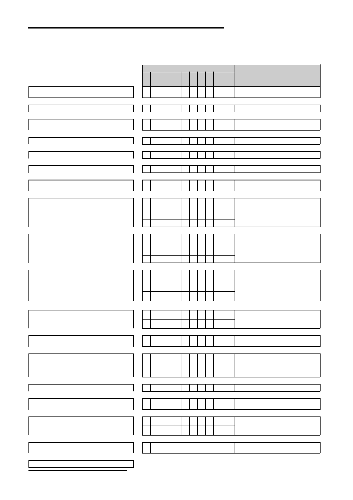
3.8 Basic Operating Sequence (example)
3.8.1 Initialization Sequence
Code Function
hex
Note
Turn on Power Supply VDD & VSS
While maintaining /RES at LOW
- - - - - - - - -
-
-
↓
Wait until power supply is stabilized
- - - - - - - - -
-
-
↓
Release the /RES Reset Signal
See AC Characteristics section
(/RES = HIGH)
- - - - - - - - -
-
for timing details
↓
LCD bias = 1/9
0 1 0 1 0 0 0 1 0
A2h
LCD panel Characteristic
↓
ADC = normal
0 1 0 1 0 0 0 0 0
A0h
No flip on x-direction (SEG)
↓
SHL = reverse
0 1 1 0 0 1 0 0 0
C8h
Flip on y-direction (COM)
↓
Initial Display Line=0
0 0 1 0 0 0 0 0 0
40h
i.e. Display RAM “page 0 - D0”
Matched to top line of the LCD
↓
Power Control
Voltage Follower = OFF
Turn on the internal Voltage
Voltage Regulator = OFF
0 0 0 1 0 1 1 0 0
2Ch
Converter and wait until VOUT
Voltage Converter = ON
stable.
Delay 50ms
- - - - - - - - -
-
↓
Power Control
Voltage Follower = OFF
Turn on the Internal Voltage
Voltage Regulator = ON
0 0 0 1 0 1 1 1 0
2Eh
Regulator and wait until VOUT
Voltage Converter = ON
stable.
Delay 50ms
- - - - - - - - -
-
↓
Power Control
Turn on the internal Voltage
Voltage Follower = ON
Follower and wait until VOUT
Voltage Regulator = ON
0 0 0 1 0 1 1 1 1
2Fh
stable
Voltage Converter = ON
Delay 50ms
- - - - - - - - -
-
↓
Booster Ratio Set
0 1 1 1 1 1 0 0 0
F8h
4x step up selected
0 0 0 0 0 0 0 0 0
00h
↓
Regulator Resistor Select
0 0 0 1 0 0 1 0 1
25h
Set the built-in resistor ratio to
middle
↓
Set to the middle of the range
Set Reference Voltage Mode
0 1 0 0 0 0 0 0 1
81h
It may be adjusted for achieving
the best display contrast
Set Reference Voltage Resistor
0 0 0 1 0 0 0 0 0
20h
↓
Display ON
0 1 0 1 0 1 1 1 1
AFh
Turn on the LCD display
↓
Set Page Address = 0
0 1 0 1 1 0 0 0 0
B0h
Specify the Display Data RAM
page address to 00h
↓
Set Column Address (Upper-4bit=0)
0 0 0 0 1 0 0 0 0
10h
Specify the Display Data RAM
Set Column Address (Lower-4bit=4)
0 0 0 0 0 0 1 0 0
04h
column address to 00h
↓
Write Display Data
1
Display Data
Write data to Display Data RAM.
↓
Write Other Display Data …
URL: www.topwaydisplay.com
Document Name: LM6060CFW-3-Manual-Rev0.1
Page: 11 of 12

TOPWAY
LCD Module User Manual
LM6060CFW-3
4. Design and Handling Precaution
Please refer to "LCD-Module-Design-Handling-Precaution.pdf".
URL: www.topwaydisplay.com
Document Name: LM6060CFW-3-Manual-Rev0.1
Page: 12 of 12