LMT050DNCFWU-NNA
LCD Module User Manual
Prepared by:
Checked by:
Approved by:
Lin Li
Date: 2018-10-18
Date:
Date:
Rev. Descriptions
Release Date
0.1
Preliminary New release
2013-11-18
0.2
Refine Section 3 Terminal Descriptions
2014-05-08
0.3
Typing correction
2016-4-5
0.4
Update section 1 and section 6
2018-10-18
URL: www.topwaydisplay.com
Document Name: LMT050DNCFWU-NNA-Manual-Rev0.4
Page: 1 of 10

TOPWAY
LCD Module User Manual
LMT050DNCFWU-NNA
Table of Content
1. General Specification ............................................................................................................... 3
1.1 Block Diagram ......................................................................................................................... 3
2. Terminal Functions ................................................................................................................... 4
2.1 Interface .................................................................................................................................... 4
3. Absolute Maximum Ratings ..................................................................................................... 4
4. Electrical Characteristics ......................................................................................................... 5
4.1 DC Characteristics (MCU terminal) ........................................................................................... 5
4.2 LED Backlight Circuit Characteristics ........................................................................................ 5
4.3 Power ON/OFF Sequence ........................................................................................................ 5
5. AC Characteristics .................................................................................................................... 7
5.1 AC Timing ................................................................................................................................. 7
5.2 Data Input format ...................................................................................................................... 8
6. Optical Characteristics ............................................................................................................. 9
7. Precautions of using LCD Modules ...................................................................................... 10
URL: www.topwaydisplay.com
Document Name: LMT050DNCFWU-NNA-Manual-Rev0.4
Page: 2 of 10
TOPWAY
LCD Module User Manual
LMT050DNCFWU-NNA
1. General Specification
Screen Size(Diagonal) :
5.0 inch
Resolution :
800 x 480
Signal Interface :
24bit parallel interface
Color Depth :
16.7M color (24bit)
Pixel Pitch :
0.135 x 0.135 (mm)
Pixel Configuration :
RGB Stripe
Display Mode :
Transmissive / normal white
Surface Treatment :
Anti-Glare Treatment
Viewing Direction :
6H (*1) (gray scale inverse)
12H (*2)
Outline Dimension :
120.7 x 75.8 x 4.1 (mm)
(exclude FPC, see attached drawing for details)
Active Area :
108 x 64.8 (mm)
Backlight :
2x7 LEDs
Operating Temperature :
-20 ~ +70°C
Storage Temperature :
-30 ~ +80°C
Note:
*1. For saturated color display content (eg. pure-red, pure-green, pure-blue, or pure-colors-combinations).
*2. For “color scales” display content.
*3. Color tone may slightly change by Temperature and Driving Condition.
1.1 Block Diagram
XL,XR
YU,YD
Touch Panel
VLED-, VLED+
Backlight Circuit
800(x3) x 480 pixels
TFT Panel
R0~R7, G0~G7, B0~B7
VDD, GND
TFT Driver
CLKIN, HSD, VSD, DEN,STBYB
URL: www.topwaydisplay.com
Document Name: LMT050DNCFWU-NNA-Manual-Rev0.4
Page: 3 of 10
TOPWAY
LCD Module User Manual
LMT050DNCFWU-NNA
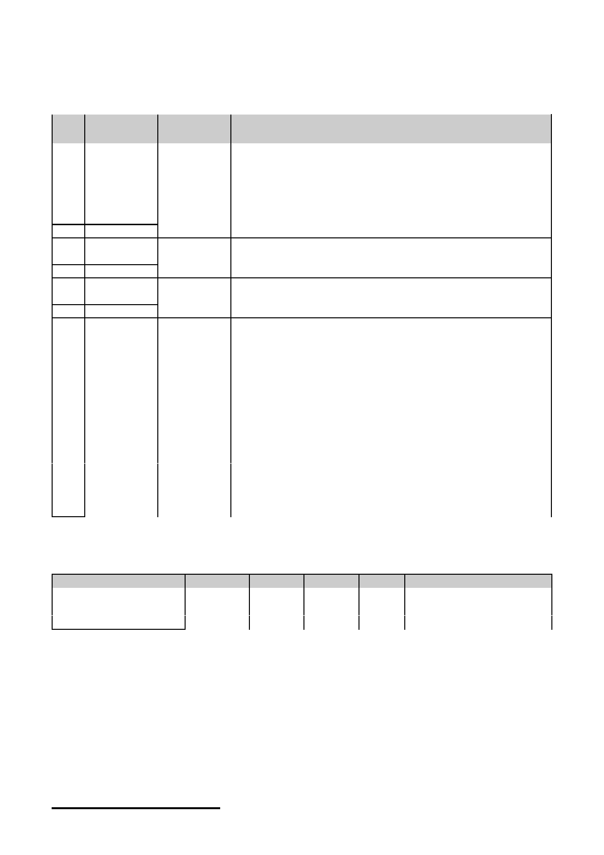
2. Terminal Functions
2.1 Interface
Pin Pin
No. Name
I/O
Descriptions
1
VLED-
Power
Backlight LED Cathode supply
2
VLED+
Power
Backlight LED Anode supply
3
GND
Power
Power Ground (0V)
4
VDD
Power
Positive Power Supply
5
R0
Input
Red color data input
:
:
12
R7
Input
13
G0
Green color data input
:
:
Input
20
G7
21
B0
Blue color data input
:
:
Input
28
B7
29
GND
Power
Power Ground (0V)
30
CLKIN
Input
Clock for input data. Data latched at falling edge of this signal.
Standby mode.
31
STBYB
Input
STBYB=“1”: Normally operation.
STBYB=“0”: Standby mode .Timing controller, source driver
will turn off, all output are High-Z.
32
HSD
Input
Horizontal Sync signal input
33
VSD
Input
Vertical Sync Signal Input
34
DEN
Input
Data input enable. DEN=1 for normal operation
35
NC
-
No connection, leave open
36
GND
Power
Power Ground (0V)
37
XR
Possitive
x-axis right side
38
YD
Possitive
y-axis down side
39
XL
Negative
x-axis left side
40
YU
Negative
y-axis upper side
Note:
Interface : HS, VS mode (default)
3. Absolute Maximum Ratings
Items
Symbol
Min.
Max.
Unit
Condition
Supply Voltage
V DD
-0.3
+4.0
V
GND = 0V
Operating Temperature
T OP
-20
+70
C
No Condensation
Storage Temperature
T ST
-30
+80
C
No Condensation
Cautions:
Any Stresses exceeding the Absolute Maximum Ratings may cause substantial damage to the device. Functional
operation of this device at other conditions beyond those listed in the specification is not implied and prolonged exposure
to extreme conditions may affect device reliability.
URL: www.topwaydisplay.com
Document Name: LMT050DNCFWU-NNA-Manual-Rev0.4
Page: 4 of 10
TOPWAY
LCD Module User Manual
LMT050DNCFWU-NNA
4. Electrical Characteristics
4.1 DC Characteristics (MCU terminal)
GND=0V, V DD =3.3V, T OP =25 C
Items
Symbol
MIN.
TYP.
MAX.
Unit Applicable Pin
Operating Voltage
VDD
3.0
3.3
3.6
V
VDD
Input High Voltage
V IH
0.7VDD
-
VDD
V
Input pins
Input Low Voltage
V IL
GND
-
0.3VDD
V
Input pins
Output Signal Low Voltage
V oH
-
-
GND+0.4
V
Output Signal High Voltage
V IL
VDD-0.4
-
-
V
Operating Current (*1)
I DD
-
TBD
-
mA
All black
Note.
*1. For different LCM, the value may have a bit of difference.
*2. To test the current dissipation, use “all Black Pattern”.
4.2 LED Backlight Circuit Characteristics
If VLED+ =40mA, T OP =25 C
Items
Symbol
MIN.
TYP.
MAX.
Unit Note
Forward Voltage
Vf
-
21.7
-
V
Forward Current
If VLED+
-
40
50
mA
Life Time
-
10,000
(20,000)
-
hr
Cautions:
Exceeding the recommended driving current could cause substantial damage to the backlight and shorten its lifetime.
VLED+
VLED-
No. of LEDs = 2x7 pcs
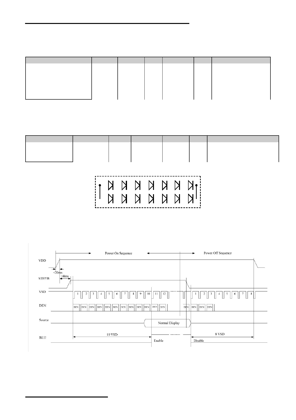
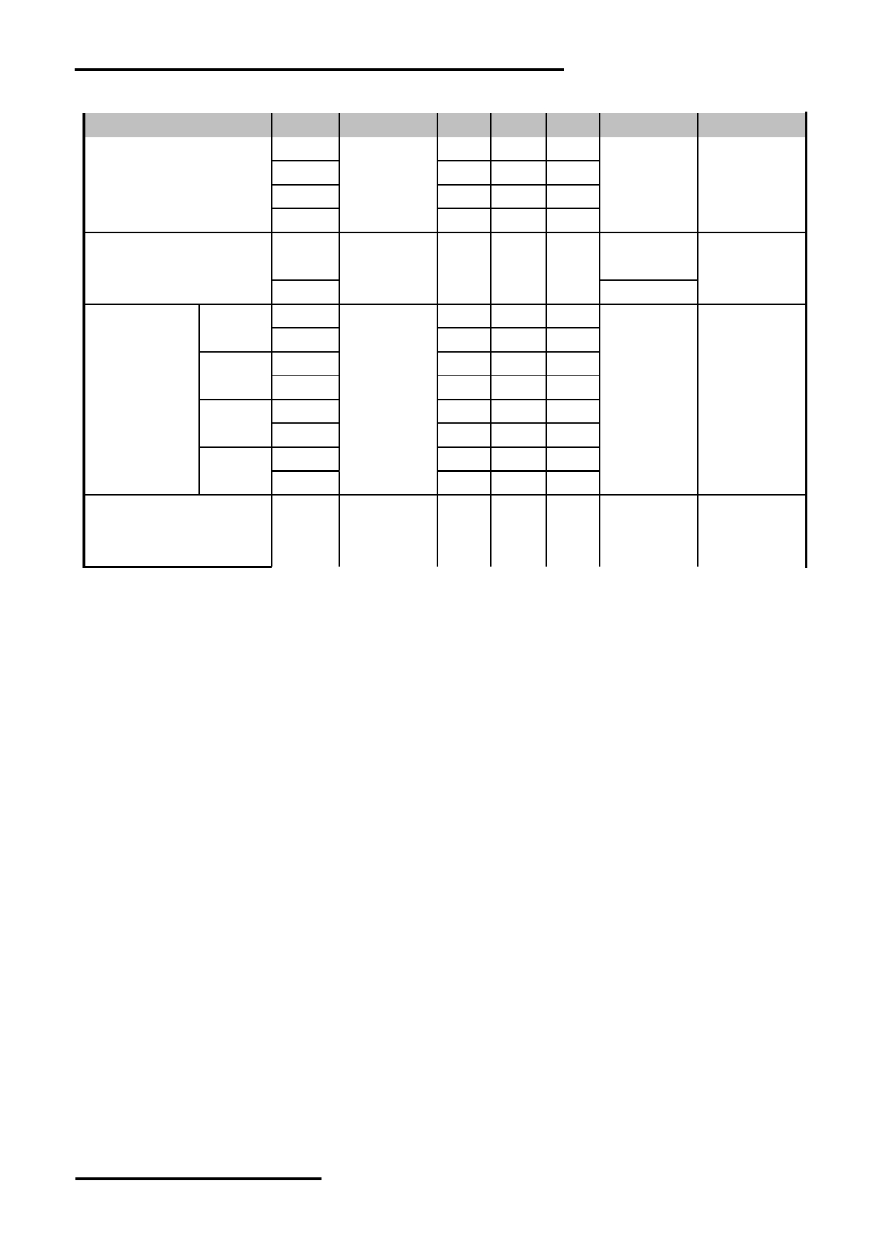
4.3 Power ON/OFF Sequence
Power On/Off Sequence
URL: www.topwaydisplay.com
Document Name: LMT050DNCFWU-NNA-Manual-Rev0.4
Page: 5 of 10

TOPWAY
LCD Module User Manual
LMT050DNCFWU-NNA
Power On Sequence
Power OFF Sequence
URL: www.topwaydisplay.com
Document Name: LMT050DNCFWU-NNA-Manual-Rev0.4
Page: 6 of 10
TOPWAY
LCD Module User Manual
LMT050DNCFWU-NNA
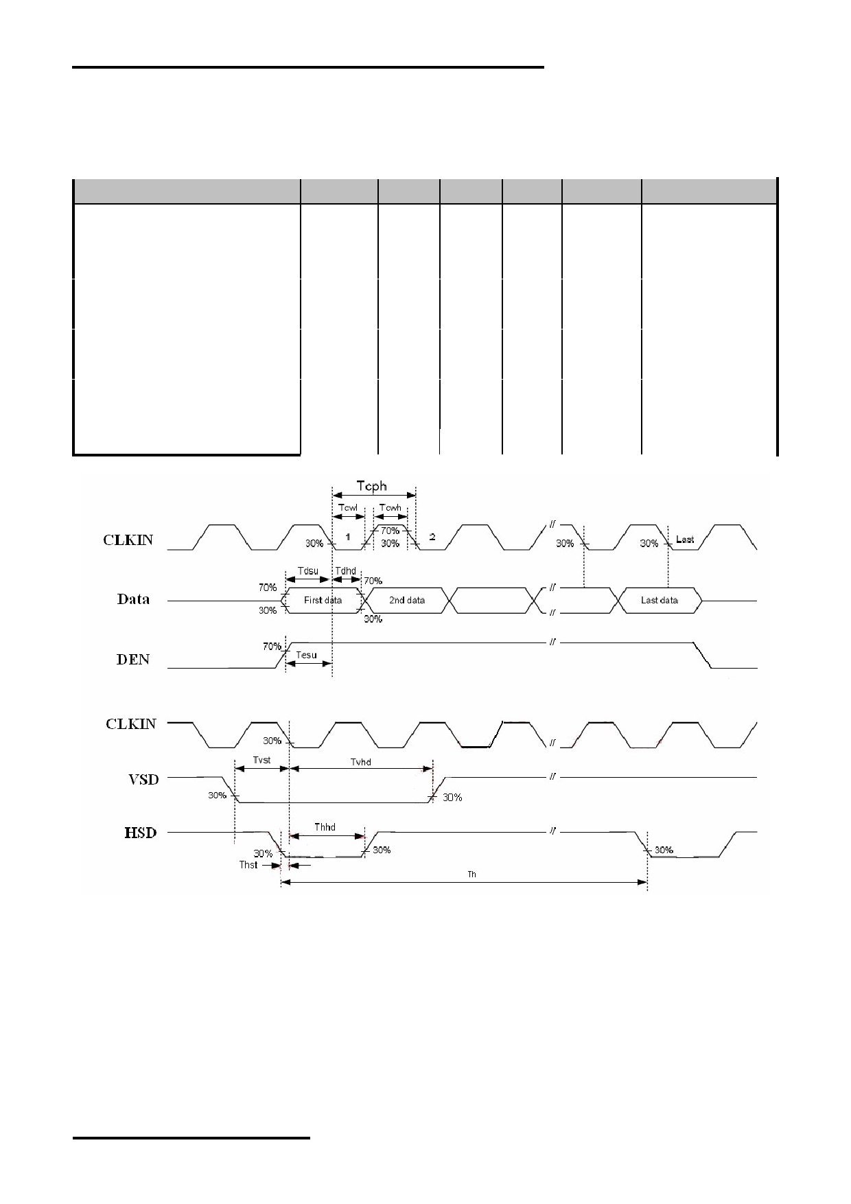
5. AC Characteristics
5.1 AC Timing
GND=0V, V DD =3.3V, T OP =25 C
Item
Symbol
MIN.
TYP.
MAX.
Unit
Remark
HS setup time
Thst
8
-
-
ns
HS hold time
Thhd
8
-
-
ns
VS setup time
Tvst
8
-
-
ns
VS hold time
Tvhd
8
-
-
ns
Data setup time
Tdsu
8
-
-
ns
Data hole time
Tdhd
8
-
-
ns
DE setup time
Tesu
8
-
-
ns
DVDD Power On Slew rate
Tpor
-
-
20
ms
CLKIN cycle time
Tcph
20
-
-
ns
CLKIN pulse duty
Tcwh
40
50
60
%
Input Clock and Data Timing Diagram
URL: www.topwaydisplay.com
Document Name: LMT050DNCFWU-NNA-Manual-Rev0.4
Page: 7 of 10
TOPWAY
LCD Module User Manual
LMT050DNCFWU-NNA
5.2 Data Input format
Item
Symbol
MIN.
TYP.
MAX.
Unit
Remark
Horizontal Display Area
thd
800
DCLK
CLKIN Frequency
fclk
-
30
50
MHz
One Horizontal Line
th
889
928
1143
CLKIN
HSD pulse width
thpw
1
48
255
CLKIN
HSD Blanking
thb
88
CLKIN
HSD Front Porch
thfp
1
40
255
CLKIN
Vertical Display Area
tvd
480
TH
VSD period time
tv
513
525
767
TH
VSD pulse width
tvpw
3
3
255
TH
VSD Blanking
tvb
32
TH
VSD Front Porch
tvfp
1
13
255
TH
Horizontal input timing diagram
Vertical input timing diagram
URL: www.topwaydisplay.com
Document Name: LMT050DNCFWU-NNA-Manual-Rev0.4
Page: 8 of 10
TOPWAY
LCD Module User Manual
LMT050DNCFWU-NNA
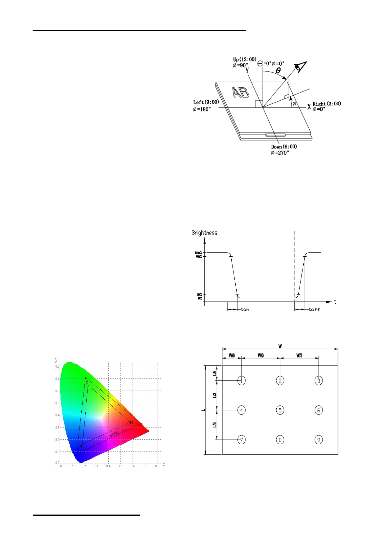
6. Optical Characteristics
Item
Symbol
Condition
MIN.
TYP.
MAX.
UNIT
Note.
θ T
40
50
-
Viewing angle
θ B
60
70
-
(CR ≥ 10)
degree
Note 2
θ L
60
70
-
θ R
60
70
-
Contrast ratio
CR
θ=0 o
500
600
-
-
Note 1,3
T on
msec
Response Time
25 ℃
-
20
30
Note 1,4
T off
msec
X
0.260 0.310 0.360
White
Y
0.280 0.330 0.380
X
0.540 0.590 0.640
Red
Y
Backlight
0.300 0.350 0.400
Chromaticlty
is on
Note 1,5
X
0.298 0.348 0.398
Green
Y
0.520 0.570 0.620
X
0.095 0.145 0.195
Blue
Y
0.060 0.110 0.160
Luminance
L
-
200
-
cd/m 2
Note 1,6
NTSC
-
50
%
Note 5
Luminance uniformity
U
75
80
-
%
Note 1,7
Test Conditions:
1. IF= 40mA, VF=21.7V, and the ambient temperature is 25. ℃
2. The test systems refer to Note 1 and Note 2.
URL: www.topwaydisplay.com
Document Name: LMT050DNCFWU-NNA-Manual-Rev0.4
Page: 9 of 10
TOPWAY
LCD Module User Manual
LMT050DNCFWU-NNA
Note 1:
Note 2:
The data are measured after LEDs are turned on for 5 minutes.
The definition of viewing angle:
LCM displays full white. The brightness is the average value of 9 Refer to the graph below marked by θ and Ф
measured spots. Measurement equipment SR-3A (1°)
Measuring condition:
- Measuring surroundings: Dark room
- Measuring temperature: Ta=25 ℃ .
- Adjust operating voltage to get optimum contrast at
the center of the display.
Note 3:
The definition of contrast ratio (Test LCM using SR-3A (1°)):
Note 4:
Contrast
Luminance When LCD is at “White” state
Definition of Response time. (Test LCD using BM-7A(2°)):
Ratio(CR)
=
Luminance When LCD is at “Black” state
The output signals of photo detector are measured
(Contrast Ratio is measured in optimum common electrode
when the input signals are changed from
voltage)
“black” to “white”(falling time)
and from “white” to “black”(rising time), respectively.
The response time is defined as
the time interval between the 10% and 90% of amplitudes.Refer to
figure as below.
Note 5:
Note 6:
Definition of Color of CIE1931 Coordinate and NTSC Ratio.
The luminance uniformity is calculated by using following formula.
△ Bp = Bp (Min.) / Bp (Max.)×100 (%)
Color gamut:
Bp (Max.) = Maximum brightness in 9 measured spots
Area of RGB triangle
S=
X100%
Bp (Min.) = Minimum brightness in 9 measured spots .
Area of NTSC triangle
Note 7:
Measured the luminance of white state at center point
7. Precautions of using LCD Modules
Please refer to "LCD-Module-Design-Handling-Precaution.pdf".
URL: www.topwaydisplay.com
Document Name: LMT050DNCFWU-NNA-Manual-Rev0.4
Page: 10 of 10