
LMT050DNCFWU-NWN
LCD Module User Manual
Prepared by:
Checked by:
Approved by:
Li KeKe
Date: 2020-08-31
Date:
Date:
Rev. Descriptions
Release Date
0.1
Preliminary
2020-08-31
URL: www.topwaydisplay.com
Document Name: LMT050DNCFWU-NWN-Manual-Rev0.1.doc
Page: 1 of 38

TOPWAY
LCD Module User Manual
LMT050DNCFWU-NWN
Table of Content
1. General Specification ............................................................................................................................... 3
2. Block Diagram ............................................................................................................................................ 3
3. Terminal Functions ................................................................................................................................... 4
3.1 Interface ...................................................................................................................................................... 4
4. Absolute Maximum Ratings .................................................................................................................... 5
5. Electrical Characteristics ........................................................................................................................ 5
5.1 DC Characteristics (MCU terminal) ........................................................................................................ 5
6. AC Characteristics .................................................................................................................................... 5
6.1 AC Timing ................................................................................................................................................... 5
6.2 TFT Controller Reset Timing ................................................................................................................. 11
6.3 Panel Setting of Timing .......................................................................................................................... 11
7. Commands ................................................................................................................................................ 12
8. Optical Characteristics .......................................................................................................................... 33
9. LCD Module Design and Handling Precautions .............................................................................. 35
10. CTP Mounting Instructions ................................................................................................................. 36
11. RTP Mounting Instructions ................................................................................................................. 37
URL: www.topwaydisplay.com
Document Name: LMT050DNCFWU-NWN-Manual-Rev0.1.doc
Page: 2 of 38
TOPWAY
LCD Module User Manual
LMT050DNCFWU-NWN
1. General Specification
Screen Size(Diagonal) :
5.0”
Outline Dimension :
136.0 x 76.0x10.3max (mm)
(see attached drawing for details)
Active Area :
108.0 x 64.8 (mm)
Color Depth:
65K Colors
Number of dots :
800 x 480
Pixel Pitch :
0.135 x 0.135 (mm)
Pixel Configuration :
RGB Stripe
Backlight :
LED
Surface Treatment :
Anti-Glare Treatment
Viewing Direction :
6H (gray scale inverse)(*2)
12H(*3)
Operating Temperature :
-20 ~ +70°C
Storage Temperature :
-30 ~ +80°C
Note:
*1 Color tune may slightly changed by temperature and driving voltage.
*2. For saturated color display content (eg. pure-red, pure-green, pure-blue, or pure-colors-combinations)
*3. For "color scales" display content
2. Block Diagram
Backlight Circuit
800 x 480 pixels
TFT Panel
/SCS, /RST, SO,SI,SCL
VDD, VSS
RA8875 or equivalent
/RST, /RD, /WR, RS, /CS, /WAIT, /INT,D0~D7
Font ROM (GT30L32S4W)
URL: www.topwaydisplay.com
Document Name: LMT050DNCFWU-NWN-Manual-Rev0.1.doc
Page: 3 of 38

TOPWAY
LCD Module User Manual
LMT050DNCFWU-NWN
3. Terminal Functions
3.1 Interface
K1,K2
Pin
Pin
I/O
4-SPI
3-SPI
I2C
No.
Name
1
VSS
P Power Ground
2
NC
-
No Connection
Reset signal
3
/RST
I
/RST = L, Initialization is executed
/RST = H, Normal running.
Chip Select
NC, please connect it to
4
/SCS
I
/CS=L, enable access to the LCD interface
/CS=H, disable access to the LCD interface
VDD.
5
SO
I/O
Data output for serial I/F.
Bi-direction data for serial
if no use, please keep
I/F
floating.
6
SI
I/O
Data input for serial I/F.
NC, please connect it to
Bi-direction data for serial
VDD.
I/F
7
SCL
I
3-wires, 4-wires Serial or IIC I/F clock.If no use, please connect it to VDD
8
VDD
P
Positive Power Supply.
K3 Pin No. Pin Name I/O
Descriptions
Note
1~2
VSS
P
Power Ground
3~4
VDD
P
Positive Power Supply
Register Select
RS = H, status read/command write
5
RS
I
cycle is selected.
RS = L, data Read/Write cycle is
selected.
Chip Select
/CS=L, enable access to the LCD
6
/CS
I
interface
/CS=H, disable access to the LCD
interface
Reset signal
7
/RST
I
/RST = L, Initialization is executed
/RST = H, Normal running.
8~15
D0~D7
I/O
Data Input
Controller busy signal output,
16
/WAIT
O
MCU should poll this signal before
accessing the LCD module
17
/INT
O
Leave Open
/WR=L H, RD=H;
18
/WR
I
Data or Instruction latch into the LCD
module
19
VSS
P
Power Ground
/WR=H, /RD=L;
20
/RD
I
Data or Status read form the LCD
module
21~26
NC
--
No Connection
URL: www.topwaydisplay.com
Document Name: LMT050DNCFWU-NWN-Manual-Rev0.1.doc
Page: 4 of 38
TOPWAY
LCD Module User Manual
LMT050DNCFWU-NWN
4. Absolute Maximum Ratings
Items
Symbol
Min.
Max.
Unit Condition
Supply Voltage
V DD
-0.3
+7.0
V
GND = 0V
Operating Temperature
T OP
-20
+70
C
No Condensation
Storage Temperature
T ST
-30
+80
C
No Condensation
Cautions:
Any Stresses exceeding the Absolute Maximum Ratings may cause substantial damage to the device. Functional
operation of this device at other conditions beyond those listed in the specification is not implied and prolonged exposure
to extreme conditions may affect device reliability.
5. Electrical Characteristics
5.1 DC Characteristics (MCU terminal)
VDD=3.3V, VSS=0V, T OP =25 C
Items
Symbol
MIN.
TYP.
MAX.
Unit Applicable Pin
Operating Voltage
VDD
3.1
3.3
3.4
V
VDD
Input High Voltage
V IH
3.0V
-
3.3
V
/RD, /WR, RS, /CS,
D0~D7, /RST,/SCS,
Input Low Voltage
V IL
VSS
-
0.5
V
SI,SCL
Output Signal High Voltage
V OH
-
-
3.3
V
D0~D7, /WAIT, /INT,SO
Output Signal Low Voltage
V OL
VSS
-
-
V
Operating Current
I DD
-
TBD
-
mA
All black, Backlight ON
-
TBD
-
mA
All black, Backlight OFF
6. AC Characteristics
6.1 AC Timing
4-Wire SPI
URL: www.topwaydisplay.com
Document Name: LMT050DNCFWU-NWN-Manual-Rev0.1.doc
Page: 5 of 38

TOPWAY
LCD Module User Manual
LMT050DNCFWU-NWN
URL: www.topwaydisplay.com
Document Name: LMT050DNCFWU-NWN-Manual-Rev0.1.doc
Page: 6 of 38
TOPWAY
LCD Module User Manual
LMT050DNCFWU-NWN
Note:1. Refer to the RA8875 datasheet for more details.
3-Wire SPI
URL: www.topwaydisplay.com
Document Name: LMT050DNCFWU-NWN-Manual-Rev0.1.doc
Page: 7 of 38

TOPWAY
LCD Module User Manual
LMT050DNCFWU-NWN
URL: www.topwaydisplay.com
Document Name: LMT050DNCFWU-NWN-Manual-Rev0.1.doc
Page: 8 of 38
TOPWAY
LCD Module User Manual
LMT050DNCFWU-NWN
Note:1. Refer to the RA8875 datasheet for more details
I2C-BUS
URL: www.topwaydisplay.com
Document Name: LMT050DNCFWU-NWN-Manual-Rev0.1.doc
Page: 9 of 38
TOPWAY
LCD Module User Manual
LMT050DNCFWU-NWN
Note:1. Refer to the RA8875 datasheet for more details
8080-8bit
URL: www.topwaydisplay.com
Document Name: LMT050DNCFWU-NWN-Manual-Rev0.1.doc
Page: 10 of 38
TOPWAY
LCD Module User Manual
LMT050DNCFWU-NWN
VDD=3.3V, VSS=0V, TOP =25 C
Parameter
Symbol
Spec.
Unit
Description
Min.
Typ
Max.
Cycle time
t CYC8
71
-
-
Strobe Pulse width
t CCC8
28
-
-
Address setup time
t AS8
5
-
-
Address hold time
t AH8
14
-
-
tc is one system
Data setup time
t DS8
28
-
-
ns
clock period:
tc = 1/SYS_CLK
Data hold time
t DH8
14
-
-
Data output access time
t ACC8
0
-
14
Data output hold time
t OH8
0
-
14
Note:1. Refer to the RA8875 datasheet for more details.
2. SYS_CLK (System clock) = 30MHz
6.2 TFT Controller Reset Timing
VSS=0V, VDD=3.3V, T OP =25 C
Item
Symbol
MIN.
TYP.
MAX.
Unit
Reset setup time
trs
2
-
-
ms
Reset pulse
trst
0.2
-
-
ms
Reset hold time
trh
2
-
-
ms
6.3 Panel Setting of Timing
Parameter
Symbol
Spec
MIN.
TYP.
MAX.
Unit
Remark
Horizontal Display Area
thd
-
800
-
CLKIN
CLKIN Frequency(60HZ)
fclk
-
30
50
MHZ
One Horizontal Line
th
889
928
1143
CLKIN
HSD pulse width
thpw
1
48
255
CLKIN
HSD Blanking
thb
88
CLKIN
HSD Front Porch
thfp
1
40
255
CLKIN
Vertical Display Area
tvd
480
TH
VSD period time
tv
513
525
767
TH
VSD pulse width
tvpw
3
3
255
TH
VSD Blanking(tvb)
tvb
32
TH
VSD Front Porch(tvfp)
tvfp
1
13
255
TH
URL: www.topwaydisplay.com
Document Name: LMT050DNCFWU-NWN-Manual-Rev0.1.doc
Page: 11 of 38

TOPWAY
LCD Module User Manual
LMT050DNCFWU-NWN
7. Commands
REG[01h] Power and Display Control Register (PWRR)
Bit Description
Default
Access
LCD Display Off
7
0:display off.
0
RW
1:display on.
6-2 NA
0
RO
Sleep Mode
0:Normal mode.
1:Sleep mode.
Note:
1
1.There are 3 ways to wake up from sleep mode:
0
RW
Touch Panel wake up,Key Scan wake up,Software wake up.
2. When using IIC, this function is not supported.
3. When using SPI, it has its particular steps to use this
function, refer to section 6-1-2-3 please.
Software Reset
0 : No action.
0
1 : Software Reset.
0
WO
Note: The bit must be set to 1 and then set to 0 to complete
a software reset
REG[02h] Memory Read/Write Command (MRWC)
Bit
Description
Default
Access
Write Function : Memory Write Data
Data to write in memory corresponding to the setting of
MWCR1[3:2].Continuous data write cycle can be accepted in
bulk data write case.
7-0 Read Function : Memory Read Data
--
RW
Data to read from memory corresponding to the setting of
MWCR1[3:2]. Continuous data read cycle can be accepted in
bulk data read case. Note that the first data read cycle is
dummy read and need to be ignored.
REG[04h] Pixel Clock Setting Register (PCSR)
Bit
Description
Default
Access
PCLK Inversion
7
0 : PDAT is fetched at PCLK rising edge.
0
RW
1 : PDAT is fetched at PCLK falling edge.
6-2 NA
0
RO
PCLK Period Setting
pixel clock (PCLK) period setting.
1-0
00b: PCLK period = System Clock period.
01b: PCLK period = 2 times of System Clock period.
0
RW
10b: PCLK period = 4 times of System Clock period.
11b: PCLK period = 8 times of System Clock period.
URL: www.topwaydisplay.com
Document Name: LMT050DNCFWU-NWN-Manual-Rev0.1.doc
Page: 12 of 38

TOPWAY
LCD Module User Manual
LMT050DNCFWU-NWN
REG[05h] Serial Flash/ROM Configuration Register (SROC)
Bit
Description
Default
Access
Serial Flash/ROM I/F # Select
7
0: Serial Flash/ROM 0 I/F is selected.
0
RW
1: Serial Flash/ROM 1 I/F is selected.
Serial Flash/ROM Address Mode
6
0: 24 bits address mode
0
RW
This bit must set to 0 for serial flash .
Serial Flash/ROM Waveform Mode
5
Mode 0.
0
RW
Mode 3.
Serial Flash /ROM Read Cycle
4-3
00b: 4 bus no dummy cycle
01b: 5 bus 1 byte dummy cycle
0
RW
1xb: 6 bus 2 byte dummy cycle
Serial Flash /ROM Access Mode
2
0: Font mode
0
RW
1: DMA mode
Serial Flash /ROM I/F Data Latch Mode Select
1-0
0xb: Single Mode
10b: Dual Mode 0.
0
RW
11b: Dual Mode 1.
REG[06h] Serial Flash/ROM CLK Setting Register(SFCLR)
Bit
Description
Default
Access
7-2 NA
0
RO
Serial Flash/ROM Clock Frequency Setting
0xb: SFCL frequency = System clock frequency
1-0
(When DMA enable and Color depth = 256 color)
SFCL frequency = System clock frequency /2)
0
RW
10b: SFCL frequency = System clock frequency / 2
11b: SFCL frequency = System clock frequency / 4
REG[10h] System Configuration Register (SYSR)
Bit
Description
Default
Access
7-4 N/A
0
RO
Color Depth Setting
3-2 00b : 8-bpp generic TFT, i.e. 256 colors.
0
RW
1xb : 16-bpp generic TFT, i.e. 65K colors.
MCUIF Selection
1-0 00b : 8-bit MCU Interface.
0
RW
1xb : 16-bit MCU Interface.
REG[12h] GPI
Bit
Description
Default
Access
7-5 NA
0
RO
GPI[4:0] : General Purpose Input.
4-0 KEY_EN = 0: General Purpose Input from pin KIN[4:0]
NA
RO
KEY_EN = 1: NC
Note :KEY_EN : REG[C0h] bit 7
REG[13h] GPO
Bit
Description
Default
Access
7-4 NA
0
RO
GPO[3:0] : General Purpose Output
3-0 KEY_EN = 0: General Purpose Output to KOUT[3:0]
0
RW
KEY_EN = 1: NC
Note: KxY_EN : REG[C0h] bit 7
URL: www.topwaydisplay.com
Document Name: LMT050DNCFWU-NWN-Manual-Rev0.1.doc
Page: 13 of 38

TOPWAY
LCD Module User Manual
LMT050DNCFWU-NWN
REG[14h] LCD Horizontal Display Width Register (HDWR)
Bit
Description
Default
Access
7
NA
0
RO
Horizontal Dis p lay Width Setting Bit[6:0]
6-0
The register specifies the LCD panel horizontal display width
in the unit of 8 pixels resolution.
0
RW
Horizontal display width(pixels) = (HDWR + 1)x8
Not e : HDWR must be set less than 64h because that the maximum horizontal display width is 800 pixels .
REG[15h] Horizontal Non-Display Period Fine Tuning Option Register (HNDFTR)
Bit
Description
Default
Access
DE Polarity
7
0 : high active.
0
RW
1 : low active.
6-4 NA
0
RO
Horizontal N on-Display Period Fine Tuning(HNDFT) [3:0]
3-0
This register specifies the fine tuning for horizontal non-
display period; it is used to support the SYNC mode panel.
0
RW
Each level of this modulation is 2-pixel.
REG[16h] LCD Horizontal Non-Display Peri o d Register (HNDR)
Bit
Description
Default
Access
7-5 NA
0
RO
Horizontal Non-Display Period(HND P ) Bit[4:0]
4-0
This register specifies the horizontal non-display period.
Horizontal Non-Display Period (pixels)
0
RW
=(HNDR + 1)x8+(HNDFTR/2+1)x2 + 2
REG[17h] HSYNC Start Position Register (HSTR)
Bit
Description
Default
Access
7-5 NA
0
RO
HSYNC Start Position[4:0]
4-0
The starting position from the end of display area to the
beginning of HSYNC. Each level of this modulation is 8-pixel.
0
RW
HSYNC Start Position(pixels) = (HSTR + 1)x8
REG[18h] HSYNC Pulse Width Resister (HPWR)
Bit
Description
Default
Access
HSYNC Po l arity
7
0 : Low active.
0
RW
1 : High active.
6-5 NA
0
RO
HSYNC Pulse Width(HPW) [4:0]
4-0 The period width of HSYNC.
0
RW
HSYNC Pulse Width(pixels) = (HPW + 1)x8
REG[19h] LCD Vertical Display Height Register (VDHR0)
Bit
Description
Default
Access
7-0
Vertical Display Height Bit[7:0]
Vertical display Height(Line) = VDHR + 1
0
RW
REG[1Ah] LCD Vertical Display Height Register0 (VDHR1)
Bit
Description
Default
Access
7-1 NA
0
RO
0
Vertical Display Height bit[8]
Vertical Display Height(Line) = VDHR + 1
0
RW
Note : The VDHR must be set less than 1E0h, because the maximum vertical display height is 480.
URL: www.topwaydisplay.com
Document Name: LMT050DNCFWU-NWN-Manual-Rev0.1.doc
Page: 14 of 38

TOPWAY
LCD Module User Manual
LMT050DNCFWU-NWN
REG[1Bh] LCD Vertical Non-Display Period Register (VNDR0)
Bit
Description
Default
Access
7-0
Vertical N o n-Display Peri o d Bit[7:0]
Vertical Non-Display Period(Line) = (VNDR + 1)
0
RW
REG[1Ch] LCD Vertical Non-Display Period Register (VNDR1)
Bit
Description
Default
Access
7-1 NA
0
RO
0
Vertical Non-Display Period bit[8]
Vertical Non-Display Period(Line) = (VNDR + 1)
0
RW
REG[1Dh] VSYNC Start Position Register (VSTR0)
Bit
Description
Default
Access
VSYNC Start Position[7:0]
7-0
The starting position from the end of display area to the
beginning of VSYNC.
0
RW
VSYNC Start Position(Line) = (VSTR + 1)
REG[1Eh] VSYNC Start Position Register (VSTR1)
Bit
Description
Default
Access
7-1 NA
0
RO
VSYNC Start Position[8]
0
The starting from the end of display area to the beginning of
VSYNC.
0
RW
VSYNC Start Position(Line) = (VSTR + 1)
RE G[1Fh] VSYNC Pulse Width Register (VPWR)
Bit
Description
Default
Access
VSYNC Polarity
7
0 : Low active.
0
RW
1 : High active.
VSYNC Pulse Width[6:0]
6-0 The pulse width of VSYNC in lines.
0
RW
VSYNC Pulse Width(Line) = (VPWR + 1)
REG[20h] Display Configuration Register (DPCR)
Bit
Description
Default
Access
Layer Setting Control
7
0 : One layer configuration is selected.
0
RW
1 : Two layers configuration is selected.
6-4 NA
0
RO
HDIR
3
Horizontal Scan Direction, for n = SEG number.
0 : SEG0 to SEG(n-1).
0
RW
1 : SEG(n-1) to SEG0.
VDIR
2
Vertical Scan direction, for n = COM number
0 : COM0 to COM(n-1).
0
RW
1 : COM(n-1) to COM0.
1-0 NA
0
RO
URL: www.topwaydisplay.com
Document Name: LMT050DNCFWU-NWN-Manual-Rev0.1.doc
Page: 15 of 38

TOPWAY
LCD Module User Manual
LMT050DNCFWU-NWN
REG[21h] Font Control Register 0 (FNCR0)
Bit
Description
Default
Access
CGRAM/CGROM Font Selection Bit in Text Mode
0 : CGROM font is selected.
1 : CGRAM font is selected.
Note:
7
1. The bit is used to select the bit-map source when text-mode
0
RW
is active(REG[40h] bit 7 is 1), when CGRAM is
writing(REG[41h] bit 3-2 =01b), the bit must be set as “0”.
2. When CGRAM font is select, REG[21h] bit 5 must be set as
1.
6
NA
0
RO
External/Internal CGROM Selection Bit
5
0 : Internal CGROM is selected.(REG[2Fh] must bx set 00h )
1 : External CGROM is selected. (REG[2Eh] bit6 &bit7 must
0
RW
be set 0)
4-2 NA
0
RO
Font Selection for internal CGROM
When FNCR0 B7 = 0 and B5 = 0, Internal CGROM supports
the 8x16 character sets with the standard coding of ISO/IEC
8859- 1~4, which supports English and most of European
1-0
country languages.
00b : ISO/IEC 8859-1.
0
RW
01b : ISO/IEC 8859-2.
10b : ISO/IEC 8859-3.
11b : ISO/IEC 8859-4.
REG[22h] Font Control Register1 (FNCR1)
Bit
Description
Default
Access
Full Alignment Selection Bit
7
0 : Full alignment is disable.
0
RW
1 : Full alignment is enable.
Font Transparency
6
0 : Font with background color.
0
RW
1 : Font with background transparency.
5
NA
0
RO
Font Rotation
4
0 : Normal.
0
RW
1 : 90 degree display.
Horizontal Font Enlargement
00b : X1.
3-2 01b : X2.
0
RW
10b : X3.
11b : X4.
Verti c al Font Enlargement
00b : X1.
1-0 01b : X2.
0
RW
10b : X3.
11b : X4.
REG[23h] CGRAM Select Register (CGSR)
Bit
Description
Default
Access
CGRAM No.
The setting of the number of the character in CGRAM. It’s
used to write the user-defined character bitmap data into
7-0 CGRAM. 16 continuous data write cycles compete the bitmap
0
RW
writing of a 8x16 character. Note that the MWCR1 bit 3-2 must
be set as 01b(CGRAM) first. And more than 16 data write
cycles will loop back to the 1 st data and cover the bitmap.
URL: www.topwaydisplay.com
Document Name: LMT050DNCFWU-NWN-Manual-Rev0.1.doc
Page: 16 of 38

TOPWAY
LCD Module User Manual
LMT050DNCFWU-NWN
REG[24h] Horizontal Scroll Offset Register 0 (HOFS0)
Bit
Description
Default
Access
Horizontal Display Scroll Offset [7:0]
7-0 The display offset of the horizontal direction, changing the
0
RW
value will cause the effect of scrolling at horizontal direction.
REG[25h] Horizontal Scroll Offset Register 1 (HOFS1)
Bit
Description
Default
Access
7-3
NA
0
RO
Ho r izontal Display Scroll Offset [10:8]
2-0 The display offset of the horizontal direction, changing the
0
RW
value will cause the effect of scrolling at horizontal direction.
REG[26h] Vertical Scroll Offset Register 0 (VOFS0)
Bit
Description
Default
Access
Vertical Display Scroll Offset [7:0]
7-0 The display offset of the vertical direction, changing the
0
RW
value will cause the effect of scrolling at vertical direction.
REG[27h] Vertical Scroll Offset Register 1 (VOFS1)
Bit
Description
Default
Access
7-2
NA
0
RO
Vertical Display Scroll Offset [9:8]
1-0 The display offset of the v ertical direction, changing the
0
RW
value will cause the effect of scrolling at vertical direction.
REG[29h] Font Line Distance Setting Register (FLDR)
Bit
Description
Default
Access
7-5
NA
0
RO
Font Line Distance Setting
4-0 Setting the font character line distance when setting
0
RW
memory font write cursor auto move. (Unit: pixel)
REG[2Ah] Font Write Cursor Horizontal Position Register 0 (F_CURXL)
Bit
Description
Default
Access
7-0
Font Write Cursor Horizontal Position[7:0]
The setting of the horizontal cursor position for font writing.
0
RW
REG[2Bh] Font Write Cursor Horizontal Position Register 1 (F_CURXH)
Bit
Description
Default
Access
7-2
NA
0
RO
1-0
Font Write Cursor Horizontal Position[ 9 :8]
The setting of the horizontal cursor position for font writing.
0
RW
REG[2Ch] Font Write Cursor Vertical Position Register 0 (F_CURYL)
Bit
Description
Default
Access
7-0
Font Write Cursor Vertical Position[7:0]
The setting of the vertical cursor position for font writing.
0
RW
REG[2Dh] Font Write Cu r sor Vertical Position Register 1 (F_CURYH)
Bit
Description
Default
Access
7-1
NA
0
RO
0
Font Write Cursor Vertical P o sition[8]
The setting of the vertical cursor position for font writing.
0
RW
URL: www.topwaydisplay.com
Document Name: LMT050DNCFWU-NWN-Manual-Rev0.1.doc
Page: 17 of 38
TOPWAY
LCD Module User Manual
LMT050DNCFWU-NWN
REG[2Eh] Font Write Type Setting Resister
Bit
Description
Default
Access
Font Size Setting (* 1)
Full Size
Half-Size
Variable
Width
00b
16x16
8x16
NX16
01b
24x24
12x24
NX24
7-6
1Xb(* 2)
32x32
16x32
NX32
0
RW
Note:
* 1The font width indicated by “N” depends on the character
code of the FONT.
* 2 The command is invalid , GT30L24T3Y does not support
size of 32x32
Font to Font Width Setting
00h : Font width off
5-0
01h : Font to Font width = 1 pixel
02h : Font to Font width = 2 pixels
0
RW
:
3Fh : Font to Font width = 63 pixels
REG[2Fh] Serial Font ROM Setting
Bit
Description
Default
Access
GT Serial Font ROM Select
000b: GT21L16TW / GT21H16T1W
7-5
001b: GT30L16U2W
010b: GT30L24T3Y / GT30H24T3Y
0
RW
011b: GT30L24M1Z
100b: GT30L32S4W / GT30H32S4W
FONT ROM Coding Setting
For specific GT serial Font ROM, the coding method must
be set for decoding.
000b: GB2312
001b: GB12345/GB18030
4-2 010b: BIG5
0
RW
011b: UNICODE
100b: ASCII
101b: UNI-Japanese
110b: JIS0208
111b: Latin/Greek/ Cyrillic / Arabic
A SCII / Latin/Greek/ Cyrillic / Arabic Latin
A SCII
Latin/Greek/
Arabic
Cyrillic
Latin
00b
Normal
Normal
NA
1-0
0
RW
01b
Arial
Variable
Presentation
Width
forms-A
10b
Roman
NA
Forms-B
11b
Bold
NA
NA
REG[30h] Horizontal Start Point 0 of Active Window (HSAW0)
Bit
Description
Default
Access
7-0
Horizontal Start Print of active Window [7:0]
0
RW
REG[31h] Horizontal Start Point 1 of active Window (HSAW1)
Bit
Description
Default
Access
7-2
NA
0
RO
1-0 Horizontal S t art Point of Active Window [9:8]
0
RW
REG[32h] Vertical Start Point 0 o f Active Wind o w (VSAW0)
Bit
Description
Default
Access
7-0 Vertical Start Point of Active Window [7:0]
0
RW
URL: www.topwaydisplay.com
Document Name: LMT050DNCFWU-NWN-Manual-Rev0.1.doc
Page: 18 of 38

TOPWAY
LCD Module User Manual
LMT050DNCFWU-NWN
REG[33h] Vertical Start Point 1 of Active Window (VSAW1)
Bit
Description
Default
Access
7-1
NA
0
RO
0
Vertical Start Point of Active Window [8]
0
RW
REG[34h] Horizontal End Point 0 of Active Window (HEAW0)
Bit
Description
Default
Access
7-0 Horizontal End Point of Active Window [7:0]
0
RW
REG[35h] Horizontal End Point 1 of Active Window (HEAW1)
Bit
Description
Default
Access
7-2
NA
0
RO
1-0 Horizontal End Point of Active Window [9:8]
0
RW
REG[36h] Vertical End Point of Active Window 0 (VEAW0)
Bit
Description
Default
Access
7-0 Vertical End Point of Active Window [7:0]
0
RW
REG[37h] Vertical End Point of Active Window 1 (VEAW1)
Bit
Description
Default
Access
7-1 NA
0
RO
0
Vertical End Point of Active Window [8]
0
RW
REG[38h] Horizontal Start Point 0 of Scroll Window (HSSW0)
Bit
Description
Default
Access
7-0 Horizontal Start Point of Scroll Window [7:0]
0
RW
REG[39h] Horizontal Start Point 1 of Scroll Window (HSSW1)
Bit
Description
Default
Access
7-2
NA
0
RO
1-0 Horizontal Start Point of Scroll Window [9:8]
0
RW
REG[3Ah] Vertical Start Point 0 of Scroll Window (VSSW0)
Bit
Description
Default
Access
7-0 Vertical Start Point of Scroll Window [7:0]
0
RW
REG[3Bh] Vertical Start Point 1 of Scroll Window (VSSW1)
Bit
Description
Default
Access
7-1
NA
0
RO
0
Vertical Start Point of Scroll Window [8]
0
RW
REG[3Ch] Horizontal End Point 0 of Scroll Window (HESW0)
Bit
Description
Default
Access
7-0 Horizontal End Point of Scroll Window [7:0]
0
RW
REG[3Dh] Horizontal End Point 1 of Scroll Window (HESW1)
Bit
Description
Default
Access
7-2
NA
0
RO
1-0 Horizontal End Point of Scroll Window [9:8]
0
RW
REG[3Eh] Vertical End Point 0 of Scroll Window (VESW0)
Bit
Description
Default
Access
7-0
Vertical End Point of Scroll Window [7:0]
0
RW
REG[3Fh] Vertical End Point 1 of Scroll Window (VESW1)
Bit
Description
Default
Access
7-1
NA
0
RO
0
Vertical End Point of Scroll Window [8]
0
RW
URL: www.topwaydisplay.com
Document Name: LMT050DNCFWU-NWN-Manual-Rev0.1.doc
Page: 19 of 38

TOPWAY
LCD Module User Manual
LMT050DNCFWU-NWN
REG[40h] Memory Write Control Register 0 (MWCR0)
Bit
Description
Default
Access
Text Mode enable
7
0 : Graphic mode.
0
RW
1 : Text mode.
Font Write Cursor/ Memory Write Cursor Enable
6
0 : Font write cursor/ Memory Write Cursor is not visible.
0
RW
1 : Font write cursor/ Memory Write Cursor is visible.
Font Write Cursor/ Memory Write Cursor Blink Enable
5
0 : Normal display.
0
RW
1 : Blink display.
4
NA
0
RO
Memory Write Direction (Only for Graphic Mode)
00b : Left Right then Top Down.
3-2 01b : Right Left then Top Down.
0
RW
10b : Top Down then Left Right.
11b : Down Top then Left Right.
Memory Write Cursor Auto-Increase Disable
1
0 : Cursor auto-increases when memory write.
0
RW
1 : Cursor doesn’t auto-increases when memory write.
Memory Read Cursor Auto-Increase Disable
0
0 : Cursor auto-increases when memory read.
0
RW
1 : Cursor doesn’t auto-increases when memory read.
REG[41h] Memory Write Control Register 1 (MWCR1)
Bit
Description
Default
Access
Graphic Cursor Enable
7
0 : Graphic Cursor disable.
0
RW
1 : Graphic Cursor enable.
Graphic Cursor Selection Bit
Select one from eight graphic cursor types.(000b to 111b)
000b : Graphic Cursor Set 1.
6-4 001b : Graphic Cursor Set 2.
0
RW
010b : Graphic Cursor Set 3.
: :
111b : Graphic Cursor Set 8.
Write Destination Selection
00b : Layer 1~2.
01b : CGRAM.
3-2 10b : Graphic Cursor.
0
RW
11b : Pattern.
Note : When CGRAM is selected (01b), REG[21h] bit 7 must
be set as “0”.
1
NA
0
RO
Layer No. for Read/Write Selection
When resolution =< 480x400 or color depth = 8bpp:
0
0 : Layer 1.
1 : Layer 2.
0
RW
When resolution > 480x400 and color depth > 8bpp:
NA, always writing to Layer 1.
REG[44h] Blink Time Control Register (BTCR)
Bit
Description
Default
Access
Text Blink Time Setting (Unit: Frame)
00h : 1 frame time.
01h : 2 frames time.
7-0
02h : 3 frames time.
:
0
RW
:
:
FFh : 256 frames time.
URL: www.topwaydisplay.com
Document Name: LMT050DNCFWU-NWN-Manual-Rev0.1.doc
Page: 20 of 38
TOPWAY
LCD Module User Manual
LMT050DNCFWU-NWN
REG[45h] Memory Read Cursor Direction (MRCD)
Bit
Description
Default
Access
7-2
NA
0
RO
Memory Read Direction (Only for Graphic Mode)
00b : Left Right then Top Down.
1-0 01b : Right Left then Top Down.
0
RW
10b : Top Down then Left Right.
11b : Down Top then Left Right.
REG[46h] Memory Write Cursor Horizontal Position Register 0 (CURH0)
Bit
Description
Default
Access
7-0 Memory Write Cursor Horizontal Location[7:0]
0
RW
REG[47h] Memory Write Cursor Horizontal Position Register 1 (CURH1)
Bit
Description
Default
Access
7-2
NA
0
RO
1-0 Memory Write Cursor Horizontal Location[9:8]
0
RW
REG[48h] Memory Write Cursor Vertical Position Register 0 (CURV0)
Bit
Description
Default
Access
7-0
Memory Write Cursor Vertical Location[7:0]
0
RW
REG[49h] Memory Write Cursor Vertical Position Register 1 (CURV1)
Bit
Description
Default
Access
7-1
NA
0
RO
0
Memory Write Cursor Vertical Location[8]
0
RW
REG[4Ah] Memory Read Cursor Horizontal Position Register 0 (RCURH0)
Bit
Description
Default
Access
7-0
Memory Read Cursor Horizontal Location[7:0]
0
RW
REG[4Bh] Memory Read Cursor Horizontal Position Register 1 (RCURH01)
Bit
Description
Default
Access
7-2
NA
0
RO
1-0 Memory Read Cursor Horizontal Location[9:8]
0
RW
REG[4Ch] Memory Read Cursor Vertical Position Register 0 (RCURV0)
Bit
Description
Default
Access
7-0
Memory Read Cursor Verti c al Location[7:0]
0
RW
REG[4Dh] Memory Read Cursor Vertical Position Register 1 (RCURV1)
Bit
Description
Default
Access
7-1
NA
0
RO
0
Memory Read Cursor Vertical Location[8]
0
RW
REG[4Eh] Font Write Cursor and Memory Write Cursor Horizontal Size Register (CURHS)
Bit
Description
Default
Access
7-5
NA
0
RO
Font Write Cursor Horizontal Size Setting[ 4 :0]
4-0
Unit : Pixel
Note : When font is enlarged, the cursor setting will multiply
7h
RW
the same times as the font enlargement.
URL: www.topwaydisplay.com
Document Name: LMT050DNCFWU-NWN-Manual-Rev0.1.doc
Page: 21 of 38

TOPWAY
LCD Module User Manual
LMT050DNCFWU-NWN
REG[4Fh] Font Write Cursor Vertical Size Register (CURVS)
Bit
Description
Default
Access
7-5
NA
0
RO
Font Write Cursor Vertical Size Setting[4:0]
4-0
Unit : Pixel
Note : When font is enlarged, the cursor setting will multiply
0
RW
the same times as the font enlargement.
REG[50h] BTE Function Control Register 0 (BECR0)
Bit
Description
Default
Access
BTE Function Ena b le / Status
Write
0 : No action.
7
1 : BTE function enable.
0
RW
Read
0 : BTE function is idle.
1 : BTE function is busy.
BTE Source Data Select
0 : Block mode,the Source BTE is stored as a rectangular
6
region of memory.
0
RW
1 : Linear mode, the Source BTE is stored as a continuous
block of memory.
B T E Destination Data Type Select
0 : Block mode, the Destination BTE is stored as a rectangular
5
region of memory.
0
RW
1 : Linear mode, the Destination BTE is stored as a
continuous block of memory.
4-0 NA
0
RO
REG[51h] BTE Function Control Register1 (BECR1)
Bit
Description
Default
Access
BTE ROP Code Bit[3:0]
7-5
ROP is the acronym for Raster Operation. Some of BTE
operation code has to collocate with ROP for the detailed
0
RW
function. (Please refer to the Section 7-6)
BTE Operation Code Bit[3:0]
RA8875 includes a 2D BTE Engine, it can execute 13 BTE
4-0
functions, the operation code range is from 1100b to 0000b
and 1111b to 1101b are not used. Some of BTE Operation
0
RW
Code has to collocate with the ROP code for the advance
function. (Please refer to the Section 7-6)
REG[68h] Background Color Register for Transparent 1 (BGTR1)
Bit
Description
Default
Access
7-6 NA
0
RO
Foreground Color Green[5:0]
If REG[10h] Bit[3:2] is set to 256 colors, the register only uses
5-0 Bit[2:0].
0
RW
If REG[10h] Bit[3:2] is set to 65K colors, the register uses
Bit[5:0].
REG[69h] Background Color Register for Transparent 2 (BGTR2)
Bit
Description
Default
Access
7-5 NA
0
RO
Foreground Color Blue[4:0]
If REG[10h] Bit[3:2] is set to 256 colors, the register only uses
4-0 Bit[1:0].
0
RW
If REG[10h] Bit[3:2] is set to 65K colors, the register uses
Bit[4:0].
URL: www.topwaydisplay.com
Document Name: LMT050DNCFWU-NWN-Manual-Rev0.1.doc
Page: 22 of 38

TOPWAY
LCD Module User Manual
LMT050DNCFWU-NWN
REG[80h] Graphic Cursor Horizontal Position Register 0 (GCHP0)
Bit
Description
Default
Access
7-0
Graphic Cursor Horizontal Location[7:0]
0
RW
REG[81h] Graphic Cursor Horizontal Position Register 1 (GCHP1)
Bit
Description
Default
Access
7-2
NA
0
RO
1-0 Graphic Cursor Horizontal Location[9:8]
0
RW
REG[82h] Graphic Cursor Vertical Position Register 0 (GCVP0)
Bit
Description
Default
Access
7-0
Graphic Cursor Vertical Location[7:0]
0
RW
REG[83h] Graphic Cursor Vertical Position Register 1 (GCVP1)
Bit
Description
Default
Access
7-1
NA
0
RO
0
Graphic Cursor Vertical Location[8]
0
RW
REG[84h] Graphic Cursor Color 0 (GCC0)
Bit
Description
Default
Access
7-0
Gra p hic Cursor Color 0 with 256 c olors
RGB Format [7:0] = RRRGGGBB.
0
RW
REG[85h] Graphic Cursor Color 1 (GCC1)
Bit
Description
Default
Access
7-0
Graphic Cursor C o lor 1 with 2 56 Colors
RGB Format [7:0] = RRRGGGBB.
0
RW
REG[88h] PLL Control Register 1 (PLLC1)
Bit
Description
Default
Access
PLLDIVM
7
PLL Pre-driver parameter.
0 : divided by 1.
0
RW
1 : divided by 2.
6-5 NA
0
RO
PLLDIVN[4:0]
4-0 PLL input parameter, the value should be 1~31. (i.e. value 0
0
RW
is forbidden).
REG[89h] PLL Control Register 2 (PLLC2)
Bit
Description
Default
Access
7-3 NA
0
RO
PLLDIVK[2:0]
PLL Output divider
000b : divided by 1.
001b : divided by 2.
2-0
010b : divided by 4.
011b : divided by 8.
03h
RW
100b : divided by 16.
101b : divided by 32.
110b : divided by 64.
111b : divided by 128.
URL: www.topwaydisplay.com
Document Name: LMT050DNCFWU-NWN-Manual-Rev0.1.doc
Page: 23 of 38

TOPWAY
LCD Module User Manual
LMT050DNCFWU-NWN
REG[8Ah] PWM1 Control Register (P1CR)
Bit
Description
Default
Access
PWM1 Enable
7
0 : Disable, PWM1_OUT level depends on P1CR bit6.
0
RW
1 : Enable.
PWM1 Disable Level
0 : PWM1_OUT is Normal L when PWM disable or Sleep
6
mode.
1 : PWM1_OUT is Normal H when PWM disable or Sleep
0
RW
mode.
The bit is only usable when P1CR bit 4 is 0
5
Reserved
0
RO
PWM1 Function Selection
0 : PWM1 function.
4
1 : PWM1 output a fixed frequency signal and it is equal to 1
0
RW
/16 oscillator clock.
PWM1 = F OSC / 16( Note )
PWM1 Clock Source Divide Ratio
0000b : SYS_CLK / 1
1000b : SYS_CLK / 256
0001b : SYS_CLK / 2
1001b : SYS_CLK / 512
0010b : SYS_CLK / 4
1010b : SYS_CLK / 1024
0011b : SYS_CLK / 8
1011b : SYS_CLK / 2048
3-0
0100b : SYS_CLK / 16
1100b : SYS_CLK / 4096
0
RW
0101b : SYS_CLK / 32
1101b : SYS_CLK / 8192
0110b : SYS_CLK / 64
1110b : SYS_CLK / 16384
0111b : SYS_CLK / 128
1111b : SYS_CLK / 32768
For example, if the system clock is 20MHz and Bit[3:0]
=0001b, when the clock source of PWM1 is 10MHz.
Note : FOSC is the frequency of external oscillator.
REG[8Bh] PWM1 Duty cycle Register (P1DCR)
Bit
Description
Default
Access
PWM Cycle Duty Selection Bit
00h 1 / 256 Duty with PWM1 clock source.
01h 2 / 256 Duty with PWM1 clock source.
7-0
02h 3 / 256 Duty with PWM1 clock source.
:
0
RW
:
FEh 255 / 256 Duty with PWM1 clock source.
FFh 256 / 256 Duty with PWM1 clock source.
URL: www.topwaydisplay.com
Document Name: LMT050DNCFWU-NWN-Manual-Rev0.1.doc
Page: 24 of 38
TOPWAY
LCD Module User Manual
LMT050DNCFWU-NWN
REG[8Ch] PWM2 Control Register (P2CR)
Bit
Description
Default
Access
PWM2 Enable
7
0 : Disable, PWM_OUT level depends on P2CR bit6.
0
RW
1 : Enable.
PWM2 Disable Level
0 : PWM2_OUT is Normal L when PWM disable or Sleep
6
mode.
1 : PWM2_OUT is Normal H when PWM disable or Sleep
0
RW
mode.
The bit is only usable when P2CR bit 4 is 0
5
Reserved
0
RO
PWM2 Function Selection
4
0 : PWM2 function.
1 : PWM2 output a signal which is the same with system clock.
0
RW
PWM2 = SYS_CLK / 16 .
PWM2 Clock Source Divide Ratio
0000b : SYS_CLK / 1
1000b : SYS_CLK / 256
0001b : SYS_CLK / 2
1001b : SYS_CLK / 512
0010b : SYS_CLK / 4
1010b : SYS_CLK / 1024
0011b : SYS_CLK / 8
1011b : SYS_CLK / 2048
3-0
0100b : SYS_CLK / 16
1100b : SYS_CLK / 4096
0
RW
0101b : SYS_CLK / 32
1101b : SYS_CLK / 8192
0110b : SYS_CLK / 64
1110b : SYS_CLK / 16384
0111b : SYS_CLK / 128
1111b : SYS_CLK / 32768
For example, if the system clock is 20MHz and Bit[3:0]
=0010b,then the clock source of PWM2 is 5MHz.
REG[8Dh] PWM2 Control Register (P2DCR)
Bit
Description
Default
Access
PWM Cycle Duty Selection Bit
00h 1 / 256 Duty with PWM2 clock source.
01h 2 / 256 Duty with PWM2 clock source.
7-0
02h 3 / 256 Duty with PWM2 clock source.
:
0
RW
:
FEh 255 / 256 Duty with PWM2 clock source.
FFh 256 / 256 Duty with PWM2 clock source.
REG[8Eh] Memory Clear Control Register (MCLR)
Bit
Description
Default
Access
Memory Clear Function
0 : End or Stop. When write 0 to this bit RA8875 will stop
7
the Memory clear function. Or if read back this bit is
0
RW
0, it indicates than Memory clear function is complete.
1 : Start the memory clear function.
Memory Clear Area Setting
0 : Clear the full window. (Please refer to the setting of
6
REG[14h], [19h], [1Ah])
1 : Clear the active window(Please refer to the setting
0
RW
of REG[30h~37h]). The layer to be cleared is according to
the setting REG[41h] Bit0.
5-0 NA
0
RO
URL: www.topwaydisplay.com
Document Name: LMT050DNCFWU-NWN-Manual-Rev0.1.doc
Page: 25 of 38
TOPWAY
LCD Module User Manual
LMT050DNCFWU-NWN
REG[90h] Draw Line/Circle/Square Control Register (DCR)
Bit
Description
Default
Access
Draw Line/Square/Triangle Start Signal
W r ite Function
0 : Stop the drawing function.
7
1 : Start the drawing function.
0
RW
Read Function
0 : Drawing function complete.
1 : Drawing function is processing.
Draw Circle Start Signal
Write Function
0 : Stop the circle drawing function.
6
1 : Start the circle drawing function.
0
RW
Read Function
0 : Circle drawing function complete.
1 : Circle drawing function is processing.
Fill the Circle/Square/Triangle Signal
5
0 : Non fill.
0
RW
1 : Fill.
Draw Line or Square Select Signal
4
0 : Draw line.
0
RW
1 : Draw square.
3-1 NA
0
RO
Draw Triangle or Line/Square Select Signal
0
0 : Draw Line or square
0
RW
1 : Draw Triangle
REG[91h] Draw Line/square Horizontal Start Address Register0 (DLHSR0)
Bit
Description
Default
Access
7-0 Draw Line/Square Horizontal Start Address[7:0]
0
RW
REG[92h] Draw Line/Square Horizontal Start Address Register1 (DLHSR1)
Bit
Description
Default
Access
7-2 NA
0
RO
1-0 Draw Line/Square Horizontal Start Address[9:8]
0
RW
REG[93h] Draw Line/Square Vertical Start Address Register0 (DLVSR0)
Bit
Description
Default
Access
7-0 Draw Line/Square Vertical Start Address[7:0]
0
RW
REG[94h] Draw Line/Square Vertical Start Address Register1 (DLVSR1)
Bit
Description
Default
Access
7-1 NA
0
RO
0
Draw Line/square Vertical Start Address[8]
0
RW
Note: start point and end point cannot equal.
REG[95h] Draw Line/Square Horizontal End Address Register0 (DLHER0)
Bit
Description
Default
Access
7-0 Draw Line/Square Horizontal End Address[7:0]
0
RW
REG[96h] Draw Line/Square Horizontal End Address Register1 (DLHER1)
Bit
Description
Default
Access
7-2 NA
0
RO
1-0 D r aw Line/Sq u are Horizontal End Addr e ss[9:8]
0
RW
REG[97h] Draw Line/Square Vertical End Address Register0 (DLVER0)
Bit
Description
Default
Access
7-0 Draw Line/Square Vertical End Address[7:0]
0
RW
URL: www.topwaydisplay.com
Document Name: LMT050DNCFWU-NWN-Manual-Rev0.1.doc
Page: 26 of 38

TOPWAY
LCD Module User Manual
LMT050DNCFWU-NWN
REG[98h] Draw Line/Square Vertical End Address Register1 (DLVER1)
Bit
Description
Default
Access
7-1 NA
0
RO
0
Draw Line/Square Vertical End Address[8]
0
RW
Note: start point and end point cannot equal.
REG[99h] Draw Circle Center Horizontal Address Register0 (DCHR0)
Bit
Description
Default
Access
7-0
Draw Circle Center Horizontal Address[7:0]
0
RW
REG[9Ah] Draw Circle Center Horizontal Address Register1 (DCHR1)
Bit
Description
Default
Access
7-2 NA
0
RO
1-0 Draw Circle Center Horizontal Address[9:8]
0
RW
REG[9Bh] Draw Circle Center Vertical Address Register0 (DCVR0)
Bit
Description
Default
Access
7-0 Draw Circle Center Vertical Address[7:0]
0
RW
REG[9Ch] Draw Circle Center Vertical Address Register1 (DCVR1)
Bit
Description
Default
Access
7-1 NA
0
RO
0
Draw Circle Center Vertical Address[8]
0
RW
REG[9Dh] Draw Circle Radius Register (DCRR)
Bit
Description
Default
Access
7-0 Draw Circle Radius[7:0]
0
RW
REG[A0h] Draw Ellipse/Ellipse Curve/Circle Square Control Register
Bit
Description
Default
Access
Draw Ellipse/Circle Square start Signal
Write Function
0 : Stop the drawing function.
7
1 : Start the drawing function.
0
RW
Read Fun c tion
0 : Drawing function complete.
1 : Drawing function is processing.
Fill the Ellipse/Circl e S q uare Signal
6
0 : Non fill.
0
RW
1 : fill.
Draw Ellipse/ Ellipse Curve or Circle Square Select Signal
5
0 : Draw Ellipse/ Ellipse curve.(Depend on bit4)
0
RW
1 : Draw Circle Square.
Draw E l lips e or Ellipse Curve Select Signal
4
0 : Draw Ellipse
0
RW
1 : Draw Ellipse Curve
3-2 NA
0
RO
1-0 Draw Ellipse Curve Part Select(DECP)
0
RW
REG[A1h] Draw Ellipse/Circle Square Long axis Setting Register (ELL_A0)
Bit
Description
Default
Access
7-0
Draw Ellipse/Circle Square Long axis[7:0]
0
RW
REG[A2h] Draw Ellipse/Circle Square Long axis Setting Register (ELL_A1)
Bit
Description
Default
Access
7-2
NA
0
RO
1-0 Draw Ellipse/Circle Square Long axis[9:8]
0
RW
URL: www.topwaydisplay.com
Document Name: LMT050DNCFWU-NWN-Manual-Rev0.1.doc
Page: 27 of 38

TOPWAY
LCD Module User Manual
LMT050DNCFWU-NWN
REG[A3h] Draw Ellipse/Circle Square Short axis Setting Register (ELL_B0)
Bit
Description
Default
Access
7-0 Draw Ellipse/Circle Square Short axis[7:0]
0
RW
REG[A4h] Draw Ellipse/Circle Square Short axis Setting Register (ELL_B1)
Bit
Description
Default
Access
7-1 NA
0
RO
0
Draw Ellipse/Circle Square Short axis[8]
0
RW
REG[A5h] Draw Ellipse/Circle Square Center Horizontal Address Register0 (DEHR0)
Bit
Description
Default
Access
7-0 Draw Ellipse/Circle Square Center Horizontal Address[7:0]
0
RW
REG[A6h] Draw Ellipse/Circle Square Center Horizontal Address Register1 (DEHR1)
Bit
Description
Default
Access
7-2 NA
0
RO
1-0 Draw Ellipse/ C ircle Square Center Horizontal Address[9:8]
0
RW
REG[A7h] Draw Ellipse/Circle Square Center Vertical Address Register0 (DEVR0)
Bit
Description
Default
Access
7-0 Draw Ellipse/Circle Square Center Vertical Address[7:0]
0
RW
REG[A8h] Draw Ellipse/Circle Square Center Vertical Address Register1 (DEVR1)
Bit
Description
Default
Access
7-1 NA
0
RO
0
Draw Ellipse/Circle Square Center Vertical Address[8]
0
RW
REG[A9h] Draw Triangle Point 2 Horizontal Address Register0 (DTPH0)
Bit
Description
Default
Access
7-0 Draw Triangle Point 2 Horizontal Address[7:0]
0
RW
REG[AAh] Draw Triangle Point 2 Horizontal Address Register1 (DTPH1)
Bit
Description
Default
Access
7-2 NA
0
RO
1-0 Draw Triang l e Point 2 Horizontal Address[9:8]
0
RW
REG[ABh] Draw Triangle Point 2 Vertical Address Register0 (DTPV0)
Bit
Description
Default
Access
7-0 Draw Tri a ngle P oint 2 Vertical Address [ 7 :0]
0
RW
REG[ACh] Draw Triangle Point 2 Vertical Address Register1 (DTPV1)
Bit
Description
Default
Access
7-1 NA
0
RO
0
Draw Triangle Point 2 Vertical A d dress [8]
0
RW
REG[B0h] Source Starting Addr e ss REG0 (SSAR0)
Bit
Description
Default
Access
7-0 DMA Source START ADDRESS [ 7 :0]
0
RW
REG[B1h] Source Starting Address REG 1 (SSAR1)
Bit
Description
Default
Access
7-0 DMA Source START ADDRESS [15:8]
0
RW
REG[B2h] Source Starting Address REG 2 (SSAR2)
Bit
Description
Default
Access
7-0 DMA Source START ADDRESS [23:16]
0
RW
URL: www.topwaydisplay.com
Document Name: LMT050DNCFWU-NWN-Manual-Rev0.1.doc
Page: 28 of 38

TOPWAY
LCD Module User Manual
LMT050DNCFWU-NWN
REG[B4h] Block Width REG 0(BWR0) / DMA Transfer Number REG 0 (DTNR0)
Bit
Description
Default
Access
When REG[BFh] bit 1 = 0 (Continuous Mode)
7-0
DMA Transfer Number [7:0]
When REG[BFh] bit 1 = 1 (Block Mode)
0
RW
DMA Block Width [7:0]
REG[B5h] Block Width REG 1 (BWR1)
Bit
Description
Default
Access
7-2
NA
0
RO
1-0 DMA Block Width [9:8]
0
RW
REG[B6h ] Block Height REG 0(BHR0) /DMA Transfer Number REG 1 (DTNR1)
Bit
Description
Default
Access
When REG[BFh] bit 1 = 0 (Co n tinuous Mode)
7-0
DMA Transfer Number [15:8]
When REG[BFh] bit 1 = 1 (Block Mode)
0
RW
DMA Block Height [7:0]
REG[B7h] Block Height REG 1 (BHR1)
Bit
Description
Default
Access
7-2
NA
0
RO
1-0 DMA B lock Hei g ht [9:8]
0
RW
REG[ B8h] Source Picture Width REG 0(SPWR0) / DMA Transfer Number REG 2(DTNR2)
Bit
Description
Default
Access
7-3 DMA Source Picture Width [7:3]
0
RW
When REG[BFh] bit 1 = 0 (Continuous Mode)
2-0
DMA Transfer Number [18:16]
When REG[BFh] bit 1 = 1 (Block Mode)
0
RW
DMA Source Picture Width [2:0]
REG[B9h] Source Picture Width REG 1 (SPWR1)
Bit
Description
Default
Access
7-2
NA
0
RO
1-0 DMA Source Picture Width [9:8]
0
RW
REG[BFh] DMA C onfiguration REG (DMACR)
Bit
Description
Default
Access
7-2 NA
0
RO
1
DMA Continuous or Block Read/Write Select Bit
0: Continuous / 1: Block
0
RW
Write F unction DMA Start B it
0
Set to 1 by MCU and reset to 0 automatically
Read Function DMA Busy Check Bit
0
RW
0:Idle / 1:Busy
Registers REG [D0h] Floating Windows Start Address XA 0 (FWSAXA0)
Bit
Description
Default
Access
7-0 Floating Windows Start Address XA [7:0]
0
RW
REG [D1h] Floating Windows Start Address XA 1 (FWSAXA1)
Bit
Description
Default
Access
7-2 NA
0
RO
1-0 Floating Windows Start Address XA [9:8]
0
RW
REG [D2h] Floating Windows Start Address YA 0 (FWSAYA0)
Bit
Description
Default
Access
7-0 Floating Windows Start Address YA [7:0]
0
RW
URL: www.topwaydisplay.com
Document Name: LMT050DNCFWU-NWN-Manual-Rev0.1.doc
Page: 29 of 38

TOPWAY
LCD Module User Manual
LMT050DNCFWU-NWN
REG [D3h] Floating Windows Start Address YA 1 (FWSAYA1)
Bit
Description
Default
Access
7-1 NA
0
RO
0
Floating Windows Start Address YA [8]
0
RW
REG [D4h] Floating Windows Width 0 (FWW0)
Bit
Description
Default
Access
7-0 Floating Windows Width Setting [7:0]
0
RW
REG [D5h] Floating Windows Width 1 (FWW1)
Bit
Description
Default
Access
7-2 NA
0
RO
1-0 Floating Windows Width Setting [9:8]
0
RW
REG [D6h] Floating Windows Height 0 (FWH0)
Bit
Description
Default
Access
7-0 Floating Windows Height Setting[7:0]
0
RW
REG [D7h] Floating Windows Height 1 (FWH1)
Bit
Description
Default
Access
7-2 NA
0
RO
1-0 Floating Windows Height Setting [9:8]
0
RW
REG [D8h] Floating Windows Display X Address 0 (FWDXA0)
Bit
Description
Default
Access
7-0 Floating Windows Display X Address [7:0]
0
RW
REG [D9h] Floating Windows Display X Address 1 (FWDXA1)
Bit
Description
Default
Access
7-2 NA
0
RO
1-0 Floating Windows Display X Address [9:8]
0
RW
REG [DAh] Floating Windows Display Y Address 0 (FWDYA0)
Bit
Description
Default
Access
7-0 Floating Windows Display X Address [ 7 :0]
0
RW
REG [DBh] Floating Windows Display Y Address 1 (FWDYA1)
Bit
Description
Default
Access
7-1 NA
0
RO
0
Floating Windows Display Y Address [8]
0
RW
SACS_MODE REG [E0h] Serial Flash/ROM Direct Access Mode
Bit
Description
Default
Access
7-1 NA
0
RO
0: direct access mode disable, then user can use for
0
FONT/DMA mode.
0
RW
1: direct access mode enable, then FONT/DMA mode disable
SACS_ADDR REG [E1h] Serial Flash/ROM Direct Access Mode Address
Bit
Description
Default
Access
Direct access mode Address
7-0 Serial Flash/ROM have 24 bit address data, user must be write
0
WO
3 times E1 for address setting.
SACS_DATA [E2h] Serial Flash/ROM Direct Access Data Read
Bit
Description
Default
Access
7-0 Direct access mode Read Data buffer
0
RO
URL: www.topwaydisplay.com
Document Name: LMT050DNCFWU-NWN-Manual-Rev0.1.doc
Page: 30 of 38

TOPWAY
LCD Module User Manual
LMT050DNCFWU-NWN
REG[F0h] Interrupt Control Register1 (INTC1)
Bit
Description
Default
Access
7-5 NA
0
RO
KEYSCAN Interrupt Enable Bit
4
0 : Disable KEYSCAN interrupt.
0
RW
1 : Enable KEYSCAN interrupt.
DMA Interrupt Enable Bit
3
0 : Disable DMA interrupt.
0
RW
1 : Enable DMA interrupt.
Touch Panel Interrupt Enable Bit
2
0 : Disable Touch interrupt.
0
RW
1 : Enable Touch interrupt.
BTE Process complete Interrupt Enable Bit
1
0 : Disable BTE process complete interrupt.
0
RW
1 : Enable BTE process complete interrupt.
When MCU-relative BTE operation is selected(*1) and BTE
Function is Enabled(REG[50h] Bit7 = 1), this bit is used to
Enable the BTE Interrupt for MCU R/W:
0 : Disable BTE interrupt for MCU R/W.
0
1 : Enable BTE interrupt for MCU R/W.
0
RW
When the BTE Function is disabled, this bit is used to
Enable the Interrupt of Font Write Function:
0 : Disable font write interrupt.
1 : Enable font write interrupt.
No t e : 1. MCU-relative BTE operations include “Write BTE with ROP”, “Read BTE”, “Transparent Write BTE”,
“Color Expand”, “Color Expand with Transparency”.
2. Font Write Interrupt indicates the completion of the font character writing to the DDRAM.
URL: www.topwaydisplay.com
Document Name: LMT050DNCFWU-NWN-Manual-Rev0.1.doc
Page: 31 of 38

TOPWAY
LCD Module User Manual
LMT050DNCFWU-NWN
REG[F1h] Interrupt Control Register2 (INTC2)
Bit
Description
Default
Access
7-5 NA
0
RO
Write Function KEYSCAN Interrupt Clear Bit
0 : No operation.
4
1 : Clear the keyscan interrupt.
Read Function KEY S CAN Interrupt Status
0
RW
0 : No keyscan interrupt happens.
1 : Keyscan interrupt happens.
Write Function DMA Interrupt Clear Bit
0 : No operation.
3
1 : Clear the DMA interrupt.
Read Function DMA Int e rrupt Status
0
RW
0 : No DMA interrupt happens.
1 : DMA interrupt happens.
Write Function Touch Panel Interrupt Clear Bit
0 : No operation.
2
1 : Clear the touch interrupt.
Read Function Touch Panel Interrupt Status
0
RW
0 : No Touch Panel interrupt happens.
1 : Touch Panel interrupt happens.
Write Function BTE Process Complete Interrupt Clear Bit
0 : No operation.
1
1 : Clear BTE process complete interrupt.
Read Function BTE Interrupt Status
0
RW
0: No BTE process complete interrupt happens.
1: BTE process complete interrupt happens.
When MCU-relative BTE opera t ion is select e d (*1) and
BTE Function is Enabled ( REG[ 5 0h] Bit7 = 1 )
Write Function BTE Interrupt for MCU R/W Enable Bit
0 : No operation.
1 : Clear BTE MCU R/W interrupt.
Read Function BTE R/W Interrupt Status
0: No BTE interrupt for MCU R/W happens.
0
1: BTE interrupt for MCU R/W happens.
0
RW
When BTE is not Enable and Text Mode is Enable Write
Function Font Write Interrupt (*2) Enable Bit
0 : No operation.
1 : Clear font write interrupt.
Read Function Font Write Interrupt Status
0: No font write interrupt happens.
1: Font write interrupt happens.
Note:
Please refer to RA8875 data sheet for details
URL: www.topwaydisplay.com
Document Name: LMT050DNCFWU-NWN-Manual-Rev0.1.doc
Page: 32 of 38

TOPWAY
LCD Module User Manual
LMT050DNCFWU-NWN
8. Optical Characteristics
Item
Symbol
Condition
MIN.
TYP.
MAX.
UNIT
Note.
θ T
40
50
-
Viewing angle
θ B
60
70
-
(CR ≥ 10)
degree
Note 2
θ L
60
70
-
θ R
60
70
-
Contrast ratio
CR
θ=0 o
500
600
-
-
Note 1,3
T on
msec
Response Time
25 ℃
-
20
30
Note 1,4
T off
msec
X
0.260 0.310 0.360
White
Y
0.280 0.330 0.380
X
0.540 0.590 0.640
Red
Y
Backlight
0.300 0.350 0.400
Chromaticlty
is on
Note 1,5
X
0.298 0.348 0.398
Green
Y
0.520 0.570 0.620
X
0.095 0.145 0.195
Blue
Y
0.060 0.110 0.160
Luminance
L
200
250
-
cd/m 2
Note 1,6
NTSC
-
50
%
Note 5
Luminance uniformity
U
75
80
-
%
Note 1,7
Test Conditions:
1. IF= 40 mA, VF=23.1V, and the ambient temperature is 25. ℃
2. The test systems refer to Note 1 and Note 2.
URL: www.topwaydisplay.com
Document Name: LMT050DNCFWU-NWN-Manual-Rev0.1.doc
Page: 33 of 38
TOPWAY
LCD Module User Manual
LMT050DNCFWU-NWN
Note 1:
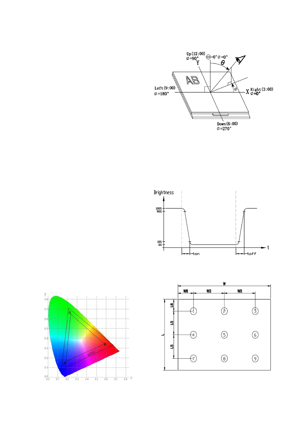
Note 2:
The data are measured after LEDs are turned on for 5 minutes.
The definition of viewing angle:
LCM displays full white. The brightness is the average value of 9 Refer to the graph below marked by θ and Ф
measured spots. Measurement equipment SR-3A (1°)
Measuring condition:
- Measuring surroundings: Dark room
- Measuring temperature: Ta=25 ℃ .
- Adjust operating voltage to get optimum contrast at
the center of the display.
Note 3:
The definition of contrast ratio (Test LCM using SR-3A (1°)):
Note 4:
Contrast
Luminance When LCD is at “White” state
Definition of Response time. (Test LCD using BM-7A(2°)):
Ratio(CR)
=
Luminance When LCD is at “Black” state
The output signals of photo detector are measured
(Contrast Ratio is measured in optimum common electrode
when the input signals are changed from
voltage)
“black” to “white”(falling time)
and from “white” to “black”(rising time), respectively.
The response time is defined as
the time interval between the 10% and 90% of amplitudes.Refer to
figure as below.
Note 5:
Note 6:
Definition of Color of CIE1931 Coordinate and NTSC Ratio.
The luminance uniformity is calculated by using following formula.
△ Bp = Bp (Min.) / Bp (Max.)×100 (%)
Color gamut:
Bp (Max.) = Maximum brightness in 9 measured spots
Area of RGB triangle
S=
X100%
Bp (Min.) = Minimum brightness in 9 measured spots .
Area of NTSC triangle
Note 7:
Measured the luminance of white state at center point
URL: www.topwaydisplay.com
Document Name: LMT050DNCFWU-NWN-Manual-Rev0.1.doc
Page: 34 of 38

TOPWAY
LCD Module User Manual
LMT050DNCFWU-NWN
9. LCD Module Design and Handling
9. 液晶显示模块设计和使用须知
Precautions
- Please ensure V0, VCOM is adjustable, to enable LCD - 请注意 V0, VCOM 的设定, 以确保液晶显示模块在
module get the best contrast ratio under different
不同的使用温度下以及在不同的视角和位置观察
temperatures, view angles and positions.
模块显示,均能达到最佳对比度,请务必将应用
电路上设置为对比度可调。
- Normally display quality should be judged under the best - 请注意液晶显示模块的显示品质判定是指在正常
contrast ratio within viewable area. Unexpected display
对比度下以及视窗(V.A)范围内进行的,非正常对
pattern may com out under abnormal contrast ratio.
比度下液晶可能会出现非预期的显示不良,应注
- Never operate the LCD module exceed the absolute
意区分。
maximum ratings.
- 请勿在最大额定值以外使用液晶显示模块。
- Never apply signal to the LCD module without power
supply.
- 请勿在没有接通电源的条件下,给液晶显示模块
输送信号。
- Keep signal line as short as possible to reduce external - 请尽可能缩短信号线的连接,以避免对液晶显示
noise interference.
模块的信号干扰。
- IC chip (e.g. TAB or COG) is sensitive to light. Strong light - 集成电路因 IC 芯片(如 TAB 或 COG)对紫外线极为
might cause malfunction. Light sealing structure casing is
敏感,强光环境下可能会引起液晶显示模块功能
recommended.
失效,故应采用不透光的外壳。
- 请在液晶显示模块与外壳之间保留足够的空间(可
- Make sure there is enough space (with cushion) between
使用衬垫),以缓冲外力对液晶显示模块的损坏或
case and LCD panel, to prevent external force passed on to
因受力不均而产生的显示不匀等异常现象。
the panel; otherwise that may cause damage to the LCD
and degrade its display result.
- 避免液晶显示屏在某一画面下长时间点亮,否则
- Avoid showing a display pattern on screen for a long time
有出现残影的风险;请通过软件每隔一段时间改
(continuous ON segment).
变一次画面。
- 液晶显示模块的可靠性可能因温度冲击而降低。
- LCD module reliability may be reduced by temperature - 请勿在阳光直射、高湿、高温或低温下储存和使
shock.
用液晶显示模块,这将造成液晶显示模块的损坏
- When storing and operating LCD module, avoids exposure
或失效。
to direct sunlight, high humidity, high or low temperature.
They may damage or degrade the LCD module.
- 请勿在极限环境(最大/最小存储/工作温度)下使
- Never leave LCD module in extreme condition (max./min
用或放置液晶显示模块超过 48 小时以上。
storage/operate temperature) for more than 48hr.
- 液 晶 显 示 模 块 建 议 存 储 条 件 为 : 0 C~40 C
- Recommend LCD module storage conditions is 0 C~40 C
<80%RH 。
<80%RH.
- 请勿让液晶显示模块存储于带有 酸性, 碱性, 有
- LCD module should be stored in the room without acid,
害气体环境之中。
alkali and harmful gas.
- 在运输过程中, 请勿让液晶显示模块跌落与猛烈
- Avoid dropping & violent shocking during transportation,
震动, 同时避免 异常挤压, 高湿度, 与阳光照
and no excessive pressure press, moisture and sunlight.
射.
- LCD module can be easily damaged by static electricity. - 液晶显示模块极易受静电损坏,请务必保证液晶
Please maintain an optimum anti-static working
显示模块在防静电的工作环境中使用或保存。
environment to protect the LCD module. (eg. ground the
(如: 烙铁正确接地,等)
soldering irons properly)
- 拿取液晶显示模块时需注意操作人员的接地情
- Be sure to ground the body when handling LCD module.
况。
- Only hold LCD module by its sides. Never hold LCD module - 请手持液晶显示模块的边沿取放模块,防止热压
by applying force on the heat seal or TAB.
纸或 TAB 部位受力。
- When soldering, control the temperature and duration avoid - 焊接液晶模块时,请注意控制烙铁的温度、焊接
damaging the backlight guide or diffuser which might
时间,以免烫坏导光板或偏光片,导致显示不匀
degrade the display result such as uneven display.
等不良现象发生。
- Never let LCD module contact with corrosive liquids, which - 请勿使用洗板水等腐蚀性液体接触液晶模块,以
might cause damage to the backlight guide or the electric
免腐蚀导光板或模块电路。
circuit of LCD module.
- Only clean LCD with a soft dry cloth, Isopropyl Alcohol or - 仅可使用柔软的干布, 异丙醇或乙醇清洁液晶屏
Ethyl Alcohol. Other solvents (e.g. water) may damage the
表面,其他任何溶剂(如:水)都有可能损坏液晶模
LCD.
块。
- Never add force to components of LCD module. It may - 请勿挤压液晶显示模块上的元器件,以避免产生
cause invisible damage or degrade the module's reliability.
潜在的损坏或失效而影响产品可靠性。
URL: www.topwaydisplay.com
Document Name: LMT050DNCFWU-NWN-Manual-Rev0.1.doc
Page: 35 of 38
TOPWAY
LCD Module User Manual
LMT050DNCFWU-NWN
- When mounting LCD module, please make sure it is free - 装配液晶显示模块时,请务必注意避免液晶显示
from twisting, warping and bending.
模块的扭曲或变形。
- Do not add excessive force on surface of LCD, which may - 请勿挤压液晶显示屏表面,这将导致显示颜色的
cause the display color change abnormally.
异常。
- LCD panel is made with glass. Any mechanical shock (e.g. - 液晶屏由玻璃制作而成,任何机械碰撞(如从高处
dropping from high place) will damage the LCD module.
跌落)均有可能损坏液晶显示模块。
- Protective film is attached on LCD screen. Be careful when - 液晶屏表面带有保护膜, 揭除保护膜时需要注意
peeling off this protective film, since static electricity may be
可能产生的静电。
generated.
- 因液晶显示屏表面的偏光片极易划伤,安装完成
- Polarizer on LCD gets scratched easily. If possible, do not
之前请尽量不要揭下保护膜。
remove LCD protective film until the last step of installation.
- 请缓慢揭除保护膜,在此过程中液晶显示屏上可
- When peeling off protective film from LCD, static charge
能会产生静电线,此为正常情况,可在短时间内
may cause abnormal display pattern. The symptom is
消失。
normal, and it will turn back to normal in a short while.
- LCD panel has sharp edges, please handle with care.
- 请注意避免被液晶显示屏的边缘割伤。
- Never attempt to disassemble or rework LCD module.
- 请不要试图拆卸或改造液晶显示模块。
- If display panel is damaged and liquid crystal substance - 当液晶显示屏出现破裂, 内部液晶液体可能流出;
leaks out, be sure not to get any in your mouth, if the
相关液体不可吞吃, 绝对不可接触嘴巴, 如接触
substance comes into contact with your skin or clothes
到皮肤或衣服, 请使用肥皂与清水彻底清洗.
promptly wash it off using soap and water.
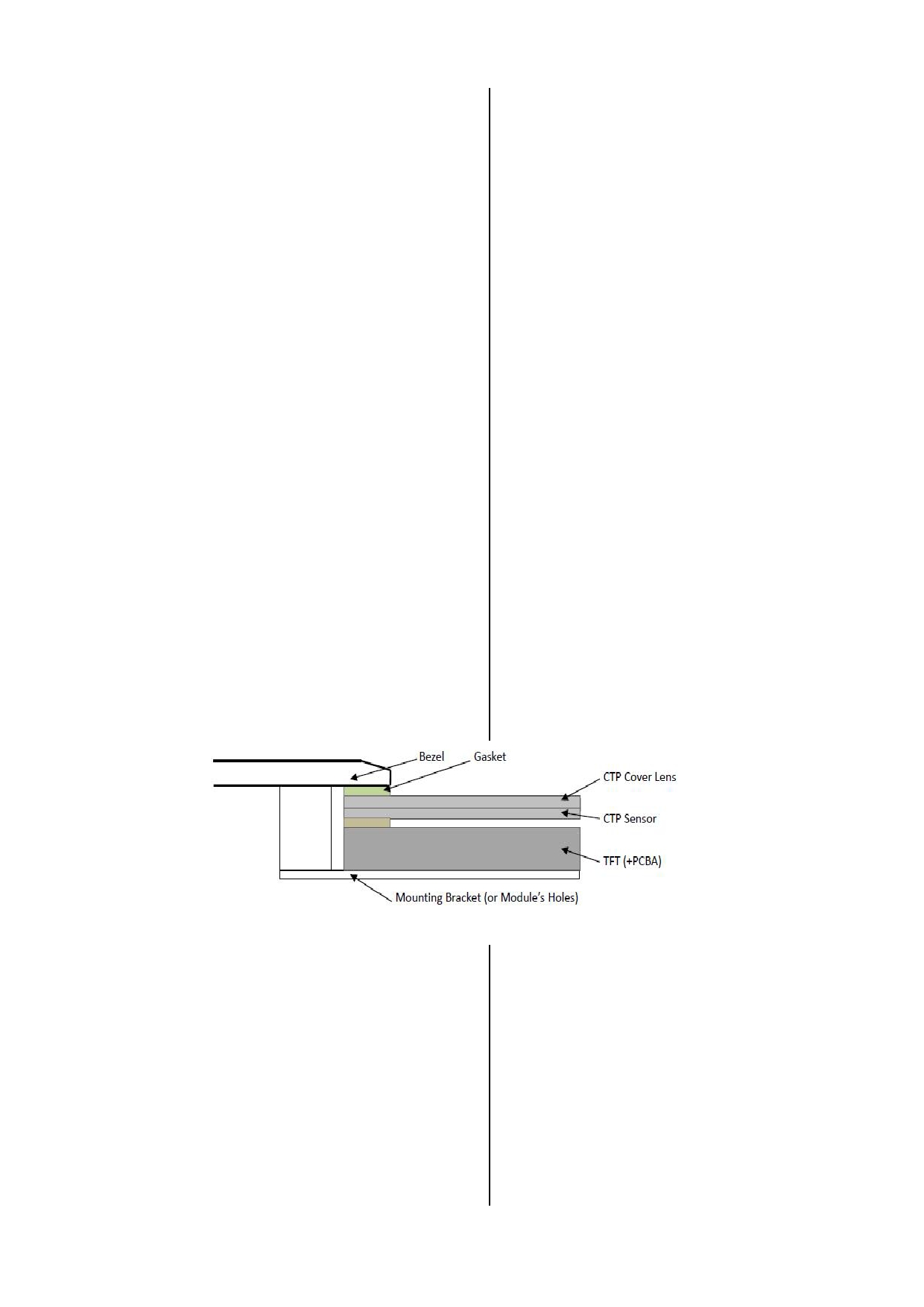
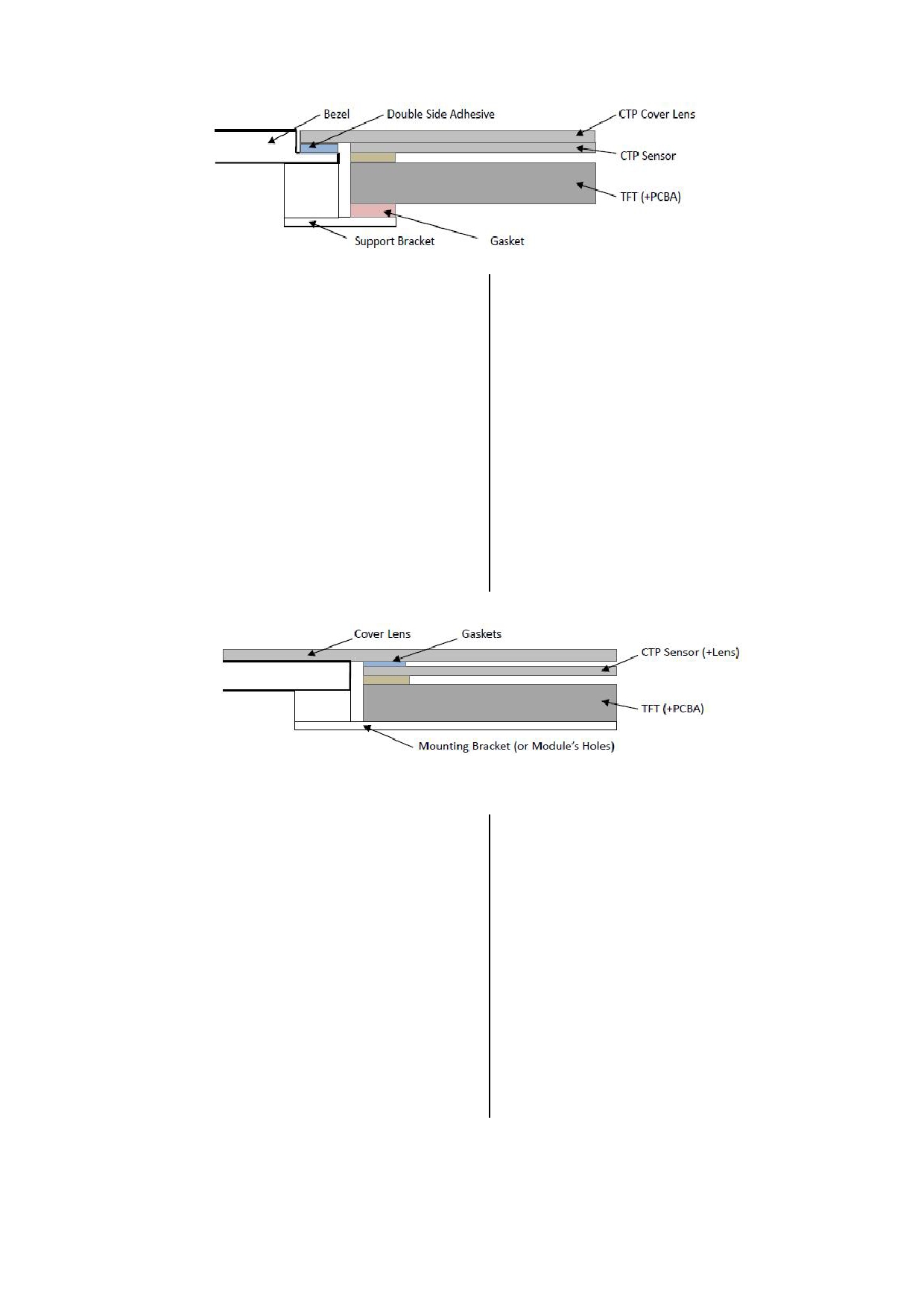
10. CTP Mounting Instructions
10. 电容触摸屏安装指导
10.1 Bezel Mounting (Figure 1)
10.1 面框安装(附图 1)
- The bezel window should be bigger than the CTP active
- 客户面框窗口应大于 CTP 动作区域,各边离动作
area. It should be ≥ 0.5mm each side.
区应≥0.5mm.
- Gasket should be installed between the bezel and the CTP
- 面框与 CTP 面板间应垫有胶垫,其最终间隙约为
surface.
0.5~1.0mm.
The final gap should be about 0.5~1.0mm.
- 建议必要时在背面提供附加支架(例如无安装结构
- It is recommended to provide an additional support bracket
的薄型 TFT 模块),应仅利用适当支撑以保持模块
for backside support when necessary (e.g. slim type TFT
位置.
module without mounding structure). They should only
provide appropriate support and keep the module in place.
- The mounting structure should be strong enough to prevent
- 安装结构应具有足够的强度,以防止外部不均匀
external uneven force or twist act onto the module.
力或扭曲力作用到模块上.
Figure 1
10.2 Surface Mounting (Figure 2)
10.2 嵌入安装(附图 2)
- As the CTP assembling on the countersink area with double - 客户面框应具有使用双面胶粘贴 CTP 的结构沉台
side
adhesive.
面,其粘贴面要求平整且洁净无污以保证粘贴牢
The countersink area should be flat and clean to ensure the
靠.
double side adhesive installation result.
- The Bezel is recommend to keep a gap ( ≥ 0.3mm each
side) around the cover lens for tolerance.
- 考虑到制作误差,建议面框与 CTP 盖板之间四周
- It is recommended to provide an additional support bracket
留有≥0.3mm 间隙.
with gasket for backside support when necessary (e.g. TFT - 建议必要时在背面提供垫有胶垫附加支架(例如无
module without mounding structure). They should only
安装结构的 TFT 模块),应仅利用适当支撑以保持
provide appropriate support and keep the module in place.
模块位置.
- The mounting structure should be strong enough to prevent
external uneven force or twist act onto the module
- 安装结构应具有足够的强度,以防止外部不均匀
力或扭曲力作用到模块上。
URL: www.topwaydisplay.com
Document Name: LMT050DNCFWU-NWN-Manual-Rev0.1.doc
Page: 36 of 38
TOPWAY
LCD Module User Manual
LMT050DNCFWU-NWN
Figure 2
10.3 Additional Cover Lens Mounting (Figure 3)
10.3 覆加盖板(附图 3)
- For the case of additional cover Lens mounting, it is - 需要覆加玻璃盖板的安装,为确保其功能,有必
necessary to recheck with the CTP specification about the
要查看产品规格书中有关盖板材料和厚度的说明.
material and thickness to ensure the functionality.
- It should keep a 0.2~0.3mm gap between the cover lens - 玻璃盖板与 CTP 表面之间应留有 0.2~0.3mm 间
and the CTP surface..
隙.
- The cover lens window should be bigger than the active
area of the CTP.It should be ≥ 0.5mm each side.
- 玻璃盖板视窗应大于 CTP 动作区域,各边离动作
- It is recommended to provide an additional support bracket
区应≥0.5mm。
for backside support when necessary (e.g. slim type TFT - 建议必要时在背面提供附加支架(例如无安装结构
module without mounding structure). They should only
的薄型 TFT 模块),应仅利用适当支撑以保持模块
provide appropriate support and keep the module in place.
位置.
- The mounting structure should be strong enough to prevent
external uneven force or twist act onto the module.
- 安装结构应具有足够的强度,以防止外部不均匀
力或扭曲力作用到模块上.
Figure 3
11. RTP Mounting Instructions
11. 电阻触摸屏安装指导
- It should bezel touching the RTP Active Area (A.A.) to
- 为避免面框直接压在动作区(A.A.)上造成误动作,
prevent abnormal touch.It should left gab D=0.2~0.3mm in
面框与电阻触摸屏(RTP)之间应留有一定的空隙
between. (Figure 4)
D=0.2~0.3mm 之间.(附图 4)
- Outer bezel design should take care about the area outside - 设计面框时,要注意用面框保护触摸屏四周的非保
the A.A. Those areas contain circuit wires which is having
证操作区域,因为布线区域在此处形成一台阶,
different thickness. Touching those areas could de-form the
在此区域附近操作时 ITO Film 变形较大,容易导
ITO film. As a result bezel the ITO film be damaged and
致 ITO 损坏而降低寿命。为保护 RTP 和避免误操
shorten its lifetime.
作,在 RTP 与面框之间垫缓冲物(Gasket),我
It is suggested to protect those areas with gasket (between
们建议设计面框应覆盖动作区的边缘,面框边缘
the bezel and RTP).The suggested figures are B≥0.50mm;
到 V.A.区的距离 B≥0.50mm; 垫圈内边缘到 V.A.
C≥0.50mm. (Figure 4)
区的距离 C≥0.50mm. (附图 4)
- The bezel side wall should keep space E= 0.2 ~ 0.3mm
- 在设计面框与 RTP 组装时,应考虑到面框内侧与
from the RTP. (Figure 4)
RTP 外侧的间距 E≥0.2mm. (附图 4)
URL: www.topwaydisplay.com
Document Name: LMT050DNCFWU-NWN-Manual-Rev0.1.doc
Page: 37 of 38
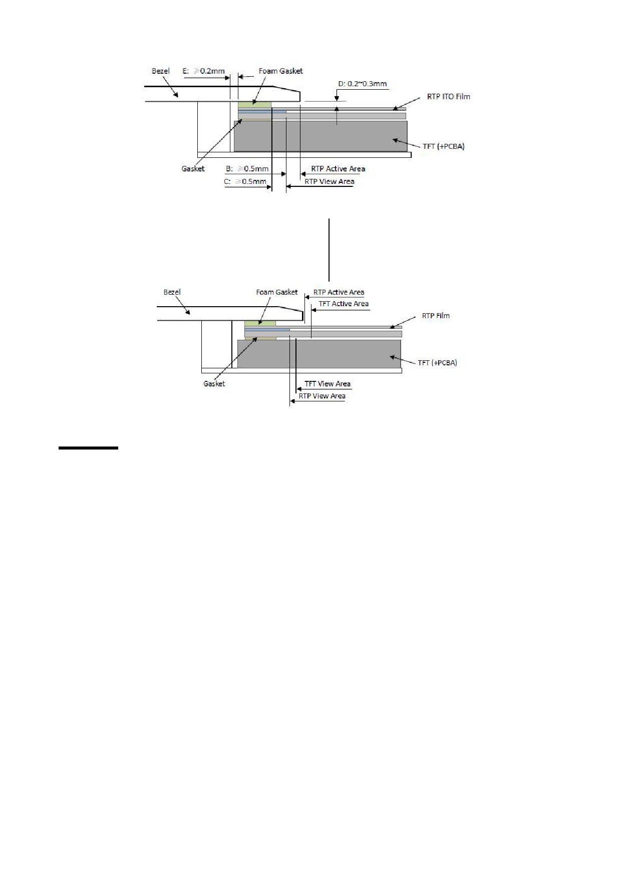
TOPWAY
LCD Module User Manual
LMT050DNCFWU-NWN
Figure 4
- In general design,
- 通常设计时:
RTP V.A. should be bigger than the TFT V.A.
RTP 的可视区 V.A. 应不小于 TFT 的可视区 V.A.
and RTP A.A. should be bigger than the TFT A.A.
及 RTP 的动作区 A.A. 应不小于 TFT 的动作区
(Figure 5)
A.A.
(附图 5)
Figure 5
Warranty
This product has been manufactured to our company’s specifications as a part for use in your company’s general
electronic products. It is guaranteed to perform according to delivery specifications. For any other use apart from
general electronic equipment, we cannot take responsibility if the product is used in medical devices, nuclear power
control equipment, aerospace equipment, fire and security systems, or any other applications in which there is a direct
risk to human life and where extremely high levels of reliability are required. If the product is to be used in any of the
above applications, we will need to enter into a separate product liability agreement.
- We cannot accept responsibility for any defect, which may arise form additional manufacturing of the product
(including disassembly and reassembly), after product delivery.
- We cannot accept responsibility for any defect, which may arise after the application of strong external force to the
product.
- We cannot accept responsibility for any defect, which may arise due to the application of static electricity after the
product has passed our company’s acceptance inspection procedures.
- When the product is in CCFL models, CCFL service life and brightness will vary according to the performance of the
inverter used, leaks, etc. We cannot accept responsibility for product performance, reliability, or defect, which may
arise.
- We cannot accept responsibility for intellectual property of a third part, which may arise through the application of
our product to our assembly with exception to those issues relating directly to the structure or method of
manufacturing of our product.
URL: www.topwaydisplay.com
Document Name: LMT050DNCFWU-NWN-Manual-Rev0.1.doc
Page: 38 of 38
