LMT050FNCFWA
LCD Module User Manual
Prepared by:
Checked by:
Approved by:
Chenzhonghua
Date: 2024-04-24
Date:
Date:
Rev.
Descriptions
Edit
Release Date
0.1
Preliminary
Chenzhonghua
2024-04-24
URL: www.topwaydisplay.com
Document Name: LMT050FNCFWA Manual-Rev0.1
Page: 1 of 17

TOPWAY
LCD Module User Manual
LMT050FNCFWA
Table of Content
1. General Specification ............................................................................................................ 3
2. Block Diagram ........................................................................................................................ 3
3. Terminal Functions ................................................................................................................ 4
3.1 Interface ............................................................................................................................... 4
4. Absolute Maximum Ratings .................................................................................................. 5
5. Electrical Characteristics ...................................................................................................... 5
5.1 DC Characteristics ............................................................................................................... 5
5.2 LED Backlight Circuit Characteristic ..................................................................................... 5
6. MIPI DC Characteristics ......................................................................................................... 6
6.1 DC Characteristics for DSI LP Mode ..................................................................................... 6
6.2 DC Characteristics for DSI HS Mode .................................................................................... 7
7. AC Characteristics ................................................................................................................. 8
7.1
MIPI DSI Timing Characteristics ........................................................................................... 8
7.1.1 High Speed Mode ...................................................................................................... 8
7.1.2 Low Power Mode ....................................................................................................... 9
7.1.3 DSI Bursts ............................................................................................................... 10
7.2 Reset Input Timing ............................................................................................................. 12
7.3 Deep Standby Mode Timing ............................................................................................... 13
8. Power On/Off Sequence ...................................................................................................... 13
9. Optical Characteristics ........................................................................................................ 14
URL: www.topwaydisplay.com
Document Name: LMT050FNCFWA Manual-Rev0.1
Page: 2 of 17

TOPWAY
LCD Module User Manual
LMT050FNCFWA
1. General Specification
Screen Size(Diagonal) :
5.0 inch
Resolution :
800(RGB) x 480
Signal Interface :
MIPI
Color Depth :
16.7M color (24bit)
Pixel Pitch :
0.135 x 0.135 (mm)
Pixel Configuration :
RGB Stripe
Display Mode :
Transmissive / normal Black
Surface Treatment :
Clear HC(3H)
Viewing Direction :
Full
Outline Dimension :
136.00x78.81x7.0 (mm)
(exclude FPC, see attached drawing for details)
Active Area :
108 x 64.8 (mm)
Backlight :
9 LEDs
Operating Temperature :
-20 ~ +70°C
Storage Temperature :
-30 ~ +80°C
Note:
*1. Color tone may slightly change by Temperature and Driving Condition.
2. Block Diagram
LEDK-, LEDA+
Backlight Circuit
800(x3) x 480 pixels
TFT Panel
D0P,D0N,D1P,D1N,D2P,D2N,D3P,D3N
VDD, GND
TFT Driver
RESET,TE,CABC,VSN,VSP,ID,CLKP,CL
KN
URL: www.topwaydisplay.com
Document Name: LMT050FNCFWA Manual-Rev0.1
Page: 3 of 17
TOPWAY
LCD Module User Manual
LMT050FNCFWA
3. Terminal Functions
3.1 Interface
Match connector type CN1: 62684-3211D0ALF
Pin No.
Pin Name
I/O
Descriptions
1
GND
P
Power Ground (0V)
2
GND
P
Power Ground (0V)
3
ID(GND)
O
ID
4
LEDK
P
Backlight LED Cathode supply
5
LEDA
p
Backlight LED Anode supply
6
NC
-
No connection
7
D0N
I
MIPI D0-
8
D0P
I
MIPI D0+
9
GND
P
Power Ground (0V)
10
D1N
I
MIPI D1-
11
D1P
I
MIPI D1+
12
GND
p
Power Ground (0V)
13
CLKN
I
MIPI CLK-
14
CLKP
I
MIPI CLK+
15
GND
P
Power Ground (0V)
16
D2N
I
MIPI D2-
17
D2P
I
MIPI D2+
18
GND
P
Power Ground (0V)
19
D3N
I
MIPI D3-
20
D3P
I
MIPI D3+
21
GND
P
Power Ground (0V)
22
IOVCC
P
Power supply(3.3v)
23
IOVCC
P
Power supply(3.3v)
24
GND
P
Power Ground (0V)
25
VSP
P
Positive Source Power
26
VSN
P
Negative Source Power
27
GND
P
Power Ground (0V)
28
CABC
O
backlight control
29
TE
O
Serves TE (Tearing Effect) pin
30
RESET
I
LCD Reset pin
31
GND
P
Power Ground (0V)
32
GND
P
Power Ground (0V)
Note: I/O Definition
I — Input, O — Output, P — Power/Ground
URL: www.topwaydisplay.com
Document Name: LMT050FNCFWA Manual-Rev0.1
Page: 4 of 17
TOPWAY
LCD Module User Manual
LMT050FNCFWA
4. Absolute Maximum Ratings
GND=0V, Ta = 25 ℃
Items
Symbol
Min.
Max.
Unit Condition
Supply Voltage
IOVCC
-0.3
+5.5
V
GND = 0V
Supply Voltage
VSP
-0.3
+6.6
V
Supply Voltage
VSN
0.3
-6.6
V
Logic Input voltage range
VIN
-0.3
IOVCC+0.3
V
Logic Output voltage range
VO
-0.3
IOVCC+0.3
V
HSSI_CLK_P/N,
HSSI_DATA0_P/N,
Differential Input voltage
HSSI_DATA1_P/N
-0.3
1.8
V
HSSI_DATA2_P/N
HSSI_DATA3_P/N
Operating Temperature
T OP
-20
+70
℃
No Condensation
Storage Temperature
T ST
-30
+80
℃
No Condensation
Cautions:
Any Stresses exceeding the Absolute Maximum Ratings may cause substantial damage to the device. Functional
operation of this device at other conditions beyond those listed in the specification is not implied and prolonged exposure
to extreme conditions may affect device reliability.
5. Electrical Characteristics
5.1 DC Characteristics
IOVCC =3.3V, GND=0V, Ta =25 ℃
Items
Symbol
MIN.
TYP.
MAX.
Unit Applicable Pin
Operating Voltage
IOVCC
3.2
3.3
3.4
V
Operating Voltage
VSP
5.4
5.5
5.6
V
Operating Voltage
VSN
-5.6
-5.5
-5.4
V
Input High Voltage
V IH
0.7 IOVCC
-
IOVCC
V
Input Low Voltage
V IL
GND
-
0.3VDD
V
Output Signal Low Voltage
V oH
0.8 IOVCC
-
IOVCC
V
Output Signal High Voltage
V OL
GND
-
0.2 IOVCC
V
Operating Current (*1)
I _IOVCC
-
25
-
mA
white pattern
5.2 LED Backlight Circuit Characteristic
I VLED =60mA, Ta=25 ℃
Items
Symbol
MIN.
TYP.
MAX.
Unit Note
Forward Voltage
VLED
8.1
9.0
9.9
V
Forward Current
I VLED
-
60
-
mA
Life Time
-
20,000
-
-
hrs
Cautions:
Exceeding the recommended driving current could cause substantial damage to the backlight and shorten its lifetime.
URL: www.topwaydisplay.com
Document Name: LMT050FNCFWA Manual-Rev0.1
Page: 5 of 17

TOPWAY
LCD Module User Manual
LMT050FNCFWA
6. MIPI DC Characteristics
6.1 DC Characteristics for DSI LP Mode
URL: www.topwaydisplay.com
Document Name: LMT050FNCFWA Manual-Rev0.1
Page: 6 of 17
TOPWAY
LCD Module User Manual
LMT050FNCFWA
6.2 DC Characteristics for DSI HS Mode
URL: www.topwaydisplay.com
Document Name: LMT050FNCFWA Manual-Rev0.1
Page: 7 of 17
TOPWAY
LCD Module User Manual
LMT050FNCFWA
7. AC Characteristics
7.1 MIPI DSI Timing Characteristics
7.1.1 High Speed Mode
URL: www.topwaydisplay.com
Document Name: LMT050FNCFWA Manual-Rev0.1
Page: 8 of 17
TOPWAY
LCD Module User Manual
LMT050FNCFWA
7.1.2 Low Power Mode
URL: www.topwaydisplay.com
Document Name: LMT050FNCFWA Manual-Rev0.1
Page: 9 of 17

TOPWAY
LCD Module User Manual
LMT050FNCFWA
7.1.3 DSI Bursts
URL: www.topwaydisplay.com
Document Name: LMT050FNCFWA Manual-Rev0.1
Page: 10 of 17
TOPWAY
LCD Module User Manual
LMT050FNCFWA
URL: www.topwaydisplay.com
Document Name: LMT050FNCFWA Manual-Rev0.1
Page: 11 of 17

TOPWAY
LCD Module User Manual
LMT050FNCFWA
7.2 Reset Input Timing
URL: www.topwaydisplay.com
Document Name: LMT050FNCFWA Manual-Rev0.1
Page: 12 of 17

TOPWAY
LCD Module User Manual
LMT050FNCFWA
7.3 Deep Standby Mode Timing
8. Power On/Off Sequence
URL: www.topwaydisplay.com
Document Name: LMT050FNCFWA Manual-Rev0.1
Page: 13 of 17
TOPWAY
LCD Module User Manual
LMT050FNCFWA
9. Optical Characteristics
Ta=25 ℃
Item
Symbol
Condition
MIN.
TYP.
MAX.
UNIT
Note.
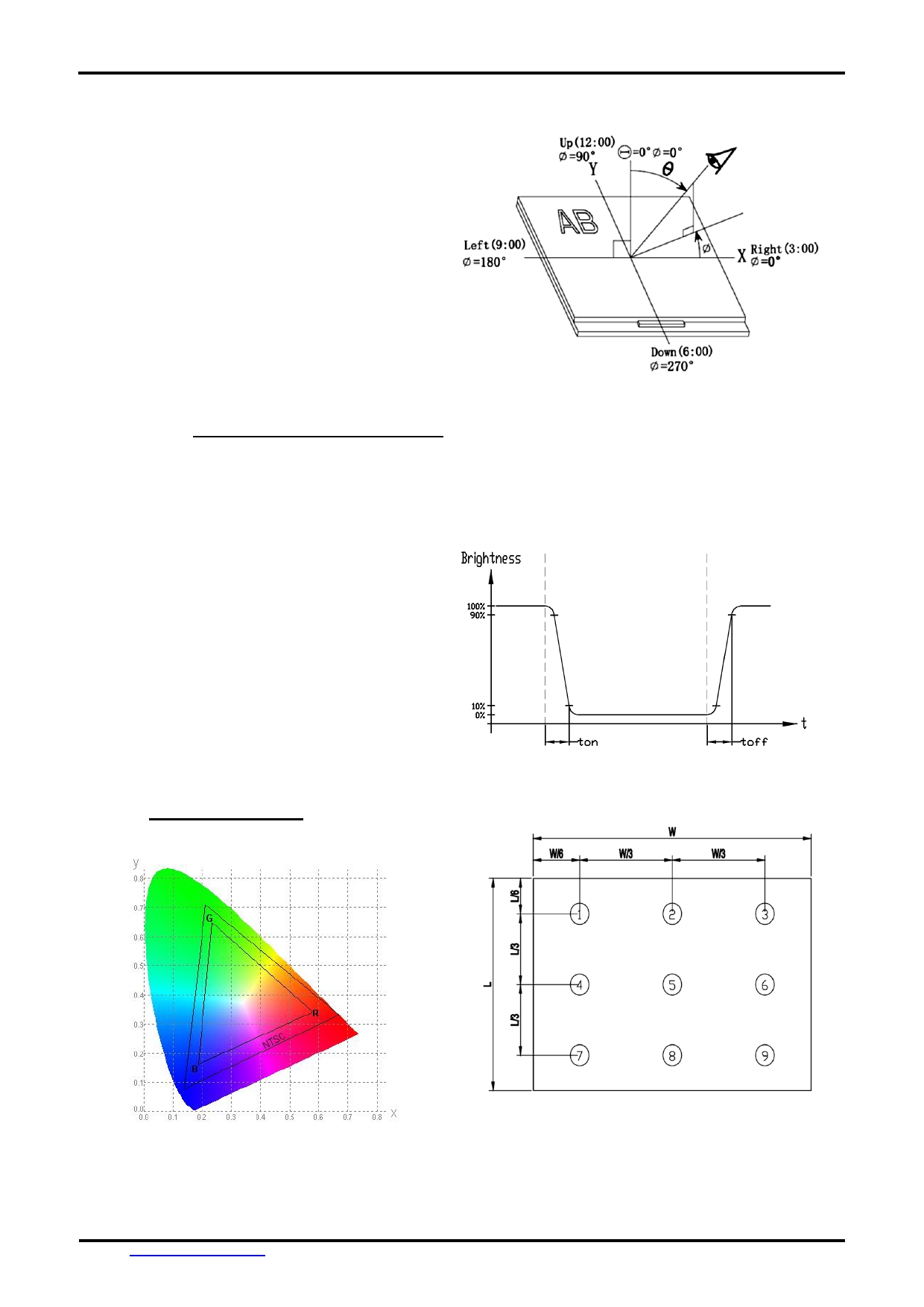
θ T
70
80
-
Viewing angle
θ B
70
80
-
(CR ≥ 10)
degree
Note 2
θ L
70
80
-
θ R
70
80
-
Contrast ratio
CR
θ =0 o
500
600
-
-
Note 1,3
T on
msec
Response Time
25 ℃
-
20
30
Note 1,4
T off
msec
X
0.259
0.309
0.359
White
Y
0.271
0.321
0.371
X
0.541
0.591
0.641
Red
Y
Backlight
0.302
0.352
0.402
Chromaticlty
is on
Note 1,5
X
0.296
0.346
0.396
Green
Y
0.529
0.579
0.629
X
0.101
0.151
0.201
Blue
Y
0.040
0.090
0.140
Luminance
L
260
350
-
cd/m 2
Note 1,6
NTSC
-
50
%
Note 5
Luminance uniformity
U
75
80
-
%
Note 1,7
Gamma
-
2.2
-
Test Conditions:
1. I_ VLED = 60mA, VLED=9.0V, and the ambient temperature is 25. ℃
2. The test systems refer to Note 1 and Note 2.
URL: www.topwaydisplay.com
Document Name: LMT050FNCFWA Manual-Rev0.1
Page: 14 of 17
TOPWAY
LCD Module User Manual
LMT050FNCFWA
Note 1:
Note 2:
The data are measured after LEDs are turned on for 5 minutes.
The definition of viewing angle:
LCM displays full white. The brightness is the average value of 9
Refer to the graph below marked by θ and Ф
measured spots. Measurement equipment SR-3A (1°
Measuring condition:
- Measuring surroundings: Dark room
- Measuring temperature: Ta=25 ℃ .
- Adjust operating voltage to get optimum contrast at
the center of the display.
Note 3:
The definition of contrast ratio (Test LCM using SR-3A (1°)):
Note 4:
Contrast
Luminance When LCD is at “White” state
Definition of Response time. (Test LCD using BM-7A(2°)):
Ratio(CR)
=
Luminance When LCD is at “Black” state
The output signals of photo detector are measured
(Contrast Ratio is measured in optimum common electrode
when the input signals are changed from
voltage)
“black” to “white”(falling time)
and from “white” to “black”(rising time), respectively.
The response time is defined as
the time interval between the 10% and 90% of amplitudes.Refer to
figure as below.
Note 5:
Note 6:
Definition of Color of CIE1931 Coordinate and NTSC Ratio.
The luminance uniformity is calculated by using following formula.
△ Bp = Bp (Min.) / Bp (Max.)×100 (%)
Color gamut:
Bp (Max.) = Maximum brightness in 9 measured spots
Area of RGB triangle
S=
X100%
Bp (Min.) = Minimum brightness in 9 measured spots .
Area of NTSC triangle
Note 7:
Measured the luminance of white state at center point
URL: www.topwaydisplay.com
Document Name: LMT050FNCFWA Manual-Rev0.1
Page: 15 of 17

TOPWAY
LCD Module User Manual
LMT050FNCFWA
Warranty
LCD Module Design and Handling Precaution
液晶显示模块设计和使用须知
-
Please ensure V0, VCOM is adjustable, to enable LCD module get
-
请注意 V0, VCOM 的设定 , 以确保液晶显示模块在不同
the best contrast ratio under different temperatures, view angles
的使用温度下以及在不同的视角和位置观察模块显示,
and positions.
均能达到最佳对比度,请务必将应用电路上设置为对比
度可调。
-
Normally display quality should be judged under the best contrast
-
请注意液晶显示模块的显示品质判定是指在正常对比度
ratio within viewable area. Unexpected display pattern may com
下以及视窗 (V.A) 范围内进行的,非正常对比度下液晶
out under abnormal contrast ratio.
可能会出现非预期的显示不良,应注意区分。
-
Never operate the LCD module exceed the absolute maximum
-
请勿在最大额定值以外使用液晶显示模块。
ratings.
-
Never apply signal to the LCD module without power supply.
-
请勿在没有接通电源的条件下,给液晶显示模块输送信
( No Hot-plugging )
号。(禁止热插拔)
-
WARNING! Be aware of (if any) frame grounding of the LCD
-
警告!使用前需评估液晶显示模块的金属框架 / 壳体地
Module connection with the system which may cause safety
( 如有 ) 与整机关系和安全性 ( 如:漏电安全性,等 ) 。
issue(e.g. electric shock,etc).
-
Keep signal line as short as possible to reduce external noise
-
请尽可能缩短信号线的连接,以避免对液晶显示模块的
interference.
信号干扰。
-
IC chip (e.g. TAB or COG) is sensitive to light. Strong light might
-
集成电路因 IC 芯片 ( 如 TAB 或 COG) 对紫外线极为敏
cause malfunction. Light sealing structure casing is recommended.
感,强光环境下可能会引起液晶显示模块功能失效,故
应采用不透光的外壳。
-
Make sure there is enough space (with cushion) between case and
-
请在液晶显示模块与外壳之间保留足够的空间 ( 可使用
LCD panel, to prevent external force passed on to the panel;
衬垫 ) ,以缓冲外力对液晶显示模块的损坏或因受力不
otherwise that may cause damage to the LCD and degrade its
均而产生的显示不匀等异常现象。
display result.
-
Avoid showing a display pattern on screen for a long time
-
避免液晶显示屏在某一画面下长时间点亮,否则有出现
(continuous ON segment).
残影的风险;请通过软件每隔一段时间改变一次画面。
-
LCD module reliability may be reduced by temperature shock.
-
液晶显示模块的可靠性可能因温度冲击而降低。
-
When storing and operating LCD module, avoids exposure to
-
请勿在阳光直射、高湿、高温或低温下储存和使用液晶
direct sunlight, high humidity, high or low temperature. They may
显示模块,这将造成液晶显示模块的损坏或失效。
damage or degrade the LCD module.
-
Never leave LCD module in extreme condition (max./min
-
请勿在极限环境 ( 最大 / 最小存储 / 工作温度 ) 下使用或放
storage/operate temperature) for more than 48hr.
置液晶显示模块超过 48 小时以上。
-
Recommend LCD module storage conditions is 0 ℃ ~40 ℃ -
液晶显示模块建议存储条件为 : 0 ℃ ~40 ℃ <80%RH 。
<80%RH.
-
LCD module should be stored in the room without acid, alkali and
-
请勿让液晶显示模块存储于带有 酸性 , 碱性 , 有害气
harmful gas.
体环境之中。
-
Avoid dropping & violent shocking during transportation, and no
-
在运输过程中 , 请勿让液晶显示模块跌落与猛烈震动 ,
excessive pressure press, moisture and sunlight.
同时避免 异常挤压 , 高湿度 , 与 阳光照射
-
LCD module can be easily damaged by static electricity. Please
-
液晶显示模块极易受静电损坏,请务必保证液晶显示模
maintain an optimum anti-static working environment to protect the
块在防静电的工作环境中使用或保存。 ( 如 : 烙铁正确
LCD module. (eg. ground the soldering irons properly)
接地 , 等 )
-
Be sure to ground the body when handling LCD module.
-
拿取液晶显示模块时需注意操作人员的接地情况。
-
Only hold LCD module by its sides. Never hold LCD module by
-
请手持液晶显示模块的边沿取放模块,防止热压纸或
applying force on the heat seal or TAB.
TAB 部位受力。
-
When soldering, control the temperature and duration avoid
-
焊接液晶模块时,请注意控制烙铁的温度、焊接时间,
damaging the backlight guide or diffuser which might degrade the
以免烫坏导光板或偏光片,导致显示不匀等不良现象发
display result such as uneven display.
生。
-
Never let LCD module contact with corrosive liquids, which might
-
请勿使用洗板水等腐蚀性液体接触液晶模块,以免腐蚀
cause damage to the backlight guide or the electric circuit of LCD
导光板或模块电路。
module.
-
Only clean LCD with a soft dry cloth, Isopropyl Alcohol or Ethyl
-
仅可使用柔软的干布 , 异丙醇或乙醇清洁液晶屏表面,
Alcohol. Other solvents (e.g. water) may damage the LCD.
其他任何溶剂 ( 如 : 水 ) 都有可能损坏液晶模块。
-
Never add force to components of LCD module. It may cause
-
请勿挤压液晶显示模块上的元器件,以避免产生潜在的
invisible damage or degrade the module's reliability.
损坏或失效而影响产品可靠性。
-
When mounting LCD module, please make sure it is free from
-
装配液晶显示模块时,请务必注意避免液晶显示模块的
twisting, warping and bending.
扭曲或变形。
-
Do not add excessive force on surface of LCD, which may cause
-
请勿挤压液晶显示屏表面,这将导致显示颜色的异常。
the display color change abnormally.
-
LCD panel is made with glass. Any mechanical shock (e.g.
-
液晶屏由玻璃制作而成,任何机械碰撞 ( 如从高处跌落 )
URL: www.topwaydisplay.com
Document Name: LMT050FNCFWA Manual-Rev0.1
Page: 16 of 17

TOPWAY
LCD Module User Manual
LMT050FNCFWA
dropping from high place) will damage the LCD module.
均有可能损坏液晶显示模块。
-
Protective film is attached on LCD screen. Be careful when peeling
-
液晶屏表面带有保护膜 , 揭除保护膜时需要注意可能产
off this protective film, since static electricity may be generated.
生的静电。
-
Polarizer on LCD gets scratched easily. If possible, do not remove
-
因液晶显示屏表面的偏光片极易划伤,安装完成之前请
LCD protective film until the last step of installation.
尽量不要揭下保护膜。
-
When peeling off protective film from LCD, static charge may
-
请缓慢揭除保护膜,在此过程中液晶显示屏上可能会产
cause abnormal display pattern. The symptom is normal, and it will
生静电线,此为正常情况,可在短时间内消失。
turn back to normal in a short while.
-
LCD panel has sharp edges, please handle with care.
-
请注意避免被液晶显示屏的边缘割伤。
-
Never attempt to disassemble or rework LCD module.
-
请不要试图拆卸或改造液晶显示模块。
-
If display panel is damaged and liquid crystal substance leaks out,
-
当液晶显示屏出现破裂 , 内部液晶液体可能流出 ; 相关
be sure not to get any in your mouth, if the substance comes into
液体不可吞吃 , 绝对不可接触嘴巴 , 如接触到皮肤或衣
contact with your skin or clothes promptly wash it off using soap
服 , 请使用肥皂与清水彻底清洗 .
and water.
URL: www.topwaydisplay.com
Document Name: LMT050FNCFWA Manual-Rev0.1
Page: 17 of 17
