
LMT056DIDFWD-AEN
LCD Module User Manual
Prepared by:
Checked by:
Approved by:
Lu jianhui
Date: 2018-02-07
Date:
Date:
Rev. Descriptions
Release Date
0.1
Preliminary
2016-12-15
0.2
Update section 2,7
2018-2-7
URL: www.topwaydisplay.com
Document Name: LMT056DIDFWD-AEN-Manual-Rev0.2
Page: 1 of 29

TOPWAY
LCD Module User Manual
LMT056DIDFWD-AEN
Table of Content
1. General Specification ............................................................................................................ 3
2. Block Diagram ........................................................................................................................ 3
3. Terminal Functions ................................................................................................................ 4
3.1
Interface ............................................................................................................................... 4
4. Absolute Maximum Ratings .................................................................................................. 5
5. Electrical Characteristics ...................................................................................................... 5
5.1
DC Characteristics (MCU terminal)....................................................................................... 5
6. AC Characteristics ................................................................................................................. 5
6.1
AC Timing ............................................................................................................................ 5
6.2
TFT Controller Reset Timing ................................................................................................ 6
6.3
Panel Setting of Timing ........................................................................................................ 6
7. Commands ............................................................................................................................. 7
8. Optical Characteristics ........................................................................................................ 28
9. Precautions of using LCD Modules .................................................................................... 29
10. Appendix <Inspection items and criteria for appearance defect> .................................... 29
URL: www.topwaydisplay.com
Document Name: LMT056DIDFWD-AEN-Manual-Rev0.2
Page: 2 of 29
TOPWAY
LCD Module User Manual
LMT056DIDFWD-AEN
1. General Specification
Screen Size(Diagonal) :
5.6”
Outline Dimension :
155.2 x 109.0 x 13.9max (mm)
(see attached drawing for details)
Active Area :
112.886 x 84.672 (mm)
Color Depth:
65k
Number of dots :
640 x 3(RGB) x 480
Pixel Pitch :
0.0588 x 0.1764 (mm)
Pixel Configuration :
RGB Stripe
Backlight :
LED
Surface Treatment :
Anti-Glare Treatment
Viewing Direction :
12H (gray scale inverse)(*2)
6H(*3)
Operating Temperature :
-20 ~ +70°C
Storage Temperature :
-30 ~ +80°C
Note:
*1 Color tune may slightly changed by temperature and driving voltage.
*2. For saturated color display content (eg. pure-red, pure-green, pure-blue, or pure-colors-combinations)
*3. For "color scales" display content
2. Block Diagram
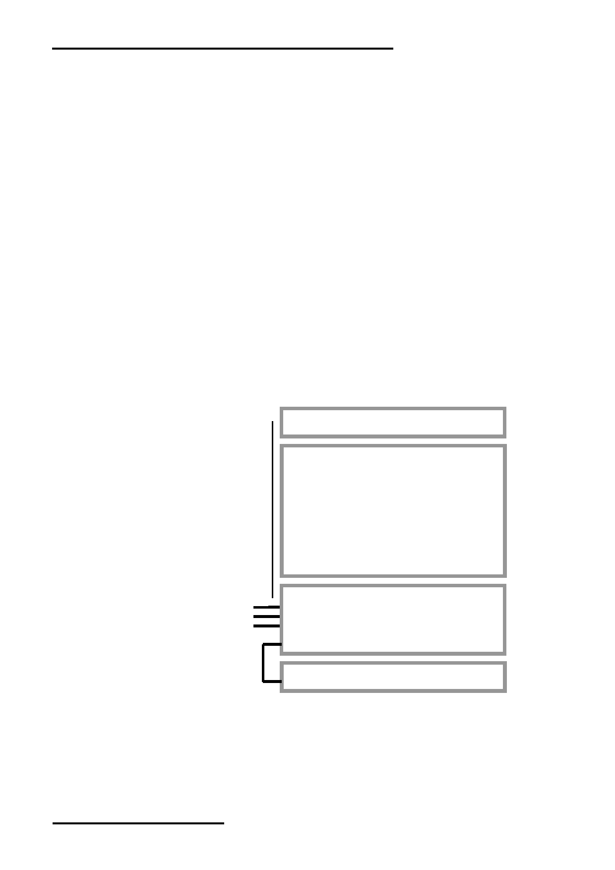
Backlight Circuit
640 x 480 pixels
TFT Panel
D0~D7
VDD, VSS
RA8875 or equivalent
D/C, /CS, /RES, TE, /RD, /WR
3.
Font ROM (GT30L24T3Y)
URL: www.topwaydisplay.com
Document Name: LMT056DIDFWD-AEN-Manual-Rev0.2
Page: 3 of 29

TOPWAY
LCD Module User Manual
LMT056DIDFWD-AEN
Terminal Functions
3.1 Interface
Pin No.
Pin Name
I/O
Descriptions
1
VSS
P
Power Ground
2
VSS
3
VDD
P
Positive Power Supply
4
VDD
Register Select
5
D/C
I
D/C = H, status read/command write cycle is selected.
D/C = L, data Read/Write cycle is selected.
Chip Select
6
/CS
I
/CS=L, enable access to the LCD interface
/CS=H, disable access to the LCD interface
Reset signal
7
/RES
I
/RES = L, Initialization is executed
/RES = H, Normal running.
8
D0
I/O
:
:
:
Data BUS
15
D7
I/O
Controller busy signal output,It is active low and could be used for
16
TE
O
MCU to pull busy status by connecting it to I/O port,
MCU should poll this signal before accessing the LCD module
/WR=H, /RD=L;
17
/RD
I
Data or Status read form the LCD module
/WR=L H, RD=H;
18
/WR
I
Data or Instruction latch into the LCD module
19
NC
--
No Connection
:
:
:
:
28
NC
--
No Connection
URL: www.topwaydisplay.com
Document Name: LMT056DIDFWD-AEN-Manual-Rev0.2
Page: 4 of 29
TOPWAY
LCD Module User Manual
LMT056DIDFWD-AEN
4. Absolute Maximum Ratings
Items
Symbol
Min.
Max.
Unit Condition
Supply Voltage
V DD
-0.3
+6.0
V
GND = 0V
Operating Temperature
T OP
-20
+70
C
No Condensation
Storage Temperature
T ST
-30
+80
C
No Condensation
Cautions:
Any Stresses exceeding the Absolute Maximum Ratings may cause substantial damage to the device. Functional
operation of this device at other conditions beyond those listed in the specification is not implied and prolonged exposure
to extreme conditions may affect device reliability.
5. Electrical Characteristics
5.1 DC Characteristics (MCU terminal)
VDD=5.0V, VSS=0V, T OP =25 C
Items
Symbol
MIN.
TYP.
MAX.
Unit Applicable Pin
Operating Voltage
VDD
4.8
5.0
5.2
V
VDD
Input High Voltage
V IH
3.0
-
VDD
V
/RD, /WR, D/C, /CS,
Input Low Voltage
V IL
0
-
0.6
V
D0~D7, /RES
Output Signal High Voltage
V OH
3.0
-
3.6
V
D0~D7, TE
Output Signal Low Voltage
V OL
0
-
0.6
V
-
450
-
mA
Backlight (100%PWM)
Operating Current
I DD
-
349
-
mA
Backlight (70%PWM)
6. AC Characteristics
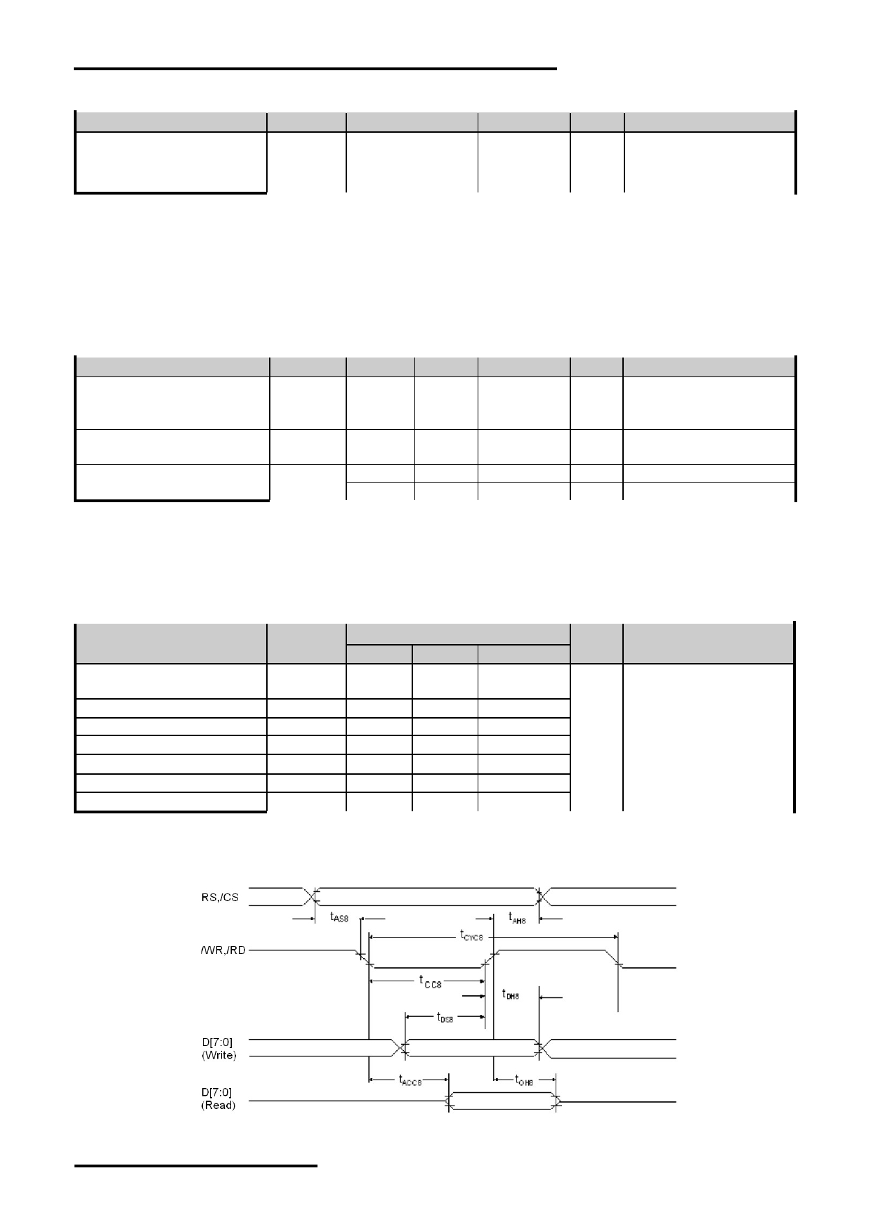
6.1 AC Timing
VDD=5.0V, VSS=0V, TOP =25 C
Parameter
Symbol
Spec.
Unit
Description
Min.
Typ
Max.
Cycle time
t CYC8
71
-
-
Strobe Pulse width
t CCC8
28
-
-
Address setup time
t AS8
5
-
-
Address hold time
t AH8
14
-
-
tc is one system
Data setup time
t DS8
28
-
-
ns
clock period:
tc = 1/SYS_CLK
Data hold time
t DH8
14
-
-
Data output access time
t ACC8
0
-
28
Data output hold time
t OH8
0
-
28
Note:1. Refer to the RA8875 datasheet for more details.
2. SYS_CLK (System clock) = 30MHz
Register Write/Read timing (for CPU 8 Bit)
URL: www.topwaydisplay.com
Document Name: LMT056DIDFWD-AEN-Manual-Rev0.2
Page: 5 of 29
TOPWAY
LCD Module User Manual
LMT056DIDFWD-AEN
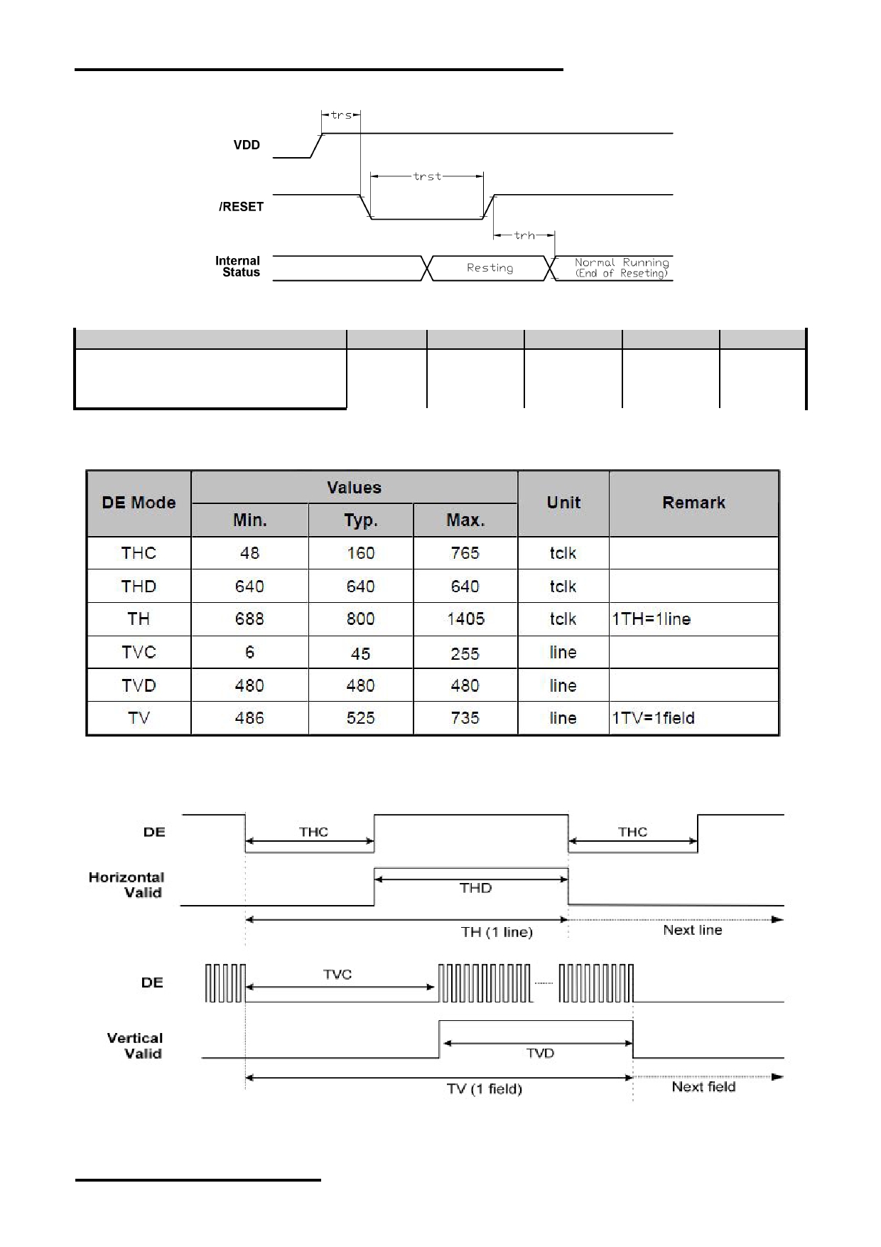
6.2 TFT Controller Reset Timing
VSS=0V, VDD=5.0V, T OP =25 C
Item
Symbol
MIN.
TYP.
MAX.
Unit
Reset setup time
trs
2
-
-
ms
Reset pulse
trst
0.2
-
-
ms
Reset hold time
trh
2
-
-
ms
6.3 Panel Setting of Timing
URL: www.topwaydisplay.com
Document Name: LMT056DIDFWD-AEN-Manual-Rev0.2
Page: 6 of 29

TOPWAY
LCD Module User Manual
LMT056DIDFWD-AEN
7. Commands
REG[01h] Power and Display Control Register (PWRR)
Bit Description
Default
Access
LCD Display Off
7
0:display off.
0
RW
1:display on.
6-2 NA
0
RO
Sleep Mode
0:Normal mode.
1:Sleep mode.
Note:
1
1.There are 3 ways to wake up from sleep mode:
0
RW
Touch Panel wake up,Key Scan wake up,Software wake up.
2. When using IIC, this function is not supported.
3. When using SPI, it has its particular steps to use this
function, refer to section 6-1-2-3 please.
Software Reset
0 : No action.
0
1 : Software Reset.
0
WO
Note: The bit must be set to 1 and then set to 0 to complete
a software reset
REG[02h] Memory Read/Write Command (MRWC)
Bit
Description
Default
Access
Write Function : Memory Write Data
Data to write in memory corresponding to the setting of
MWCR1[3:2].Continuous data write cycle can be accepted in
bulk data write case.
7-0 Read Function : Memory Read Data
--
RW
Data to read from memory corresponding to the setting of
MWCR1[3:2]. Continuous data read cycle can be accepted in
bulk data read case. Note that the first data read cycle is
dummy read and need to be ignored.
REG[04h] Pixel Clock Setting Register (PCSR)
Bit
Description
Default
Access
PCLK Inversion
7
0 : PDAT is fetched at PCLK rising edge.
0
RW
1 : PDAT is fetched at PCLK falling edge.
6-2 NA
0
RO
PCLK Period Setting
pixel clock (PCLK) period setting.
1-0
00b: PCLK period = System Clock period.
01b: PCLK period = 2 times of System Clock period.
0
RW
10b: PCLK period = 4 times of System Clock period.
11b: PCLK period = 8 times of System Clock period.
URL: www.topwaydisplay.com
Document Name: LMT056DIDFWD-AEN-Manual-Rev0.2
Page: 7 of 29
TOPWAY
LCD Module User Manual
LMT056DIDFWD-AEN
REG[05h] Serial Flash/ROM Configuration Register (SROC)
Bit
Description
Default
Access
Serial Flash/ROM I/F # Select
7
0: Serial Flash/ROM 0 I/F is selected.
0
RW
1: Serial Flash/ROM 1 I/F is selected.
Serial Flash/ROM Address Mode
6
0: 24 bits address mode
0
RW
This bit must set to 0 for serial flash .
Serial Flash/ROM Waveform Mode
5
Mode 0.
0
RW
Mode 3.
Serial Flash /ROM Read Cycle
4-3
00b: 4 bus no dummy cycle
01b: 5 bus 1 byte dummy cycle
0
RW
1xb: 6 bus 2 byte dummy cycle
Serial Flash /ROM Access Mode
2
0: Font mode
0
RW
1: DMA mode
Serial Flash /ROM I/F Data Latch Mode Select
1-0
0xb: Single Mode
10b: Dual Mode 0.
0
RW
11b: Dual Mode 1.
REG[06h] Serial Flash/ROM CLK Setting Register(SFCLR)
Bit
Description
Default
Access
7-2 NA
0
RO
Serial Flash/ROM Clock Frequency Setting
0xb: SFCL frequency = System clock frequency
1-0
(When DMA enable and Color depth = 256 color)
SFCL frequency = System clock frequency /2)
0
RW
10b: SFCL frequency = System clock frequency / 2
11b: SFCL frequency = System clock frequency / 4
REG[10h] System Configuration Register (SYSR)
Bit
Description
Default
Access
7-4 N/A
0
RO
Color Depth Setting
3-2 00b : 8-bpp generic TFT, i.e. 256 colors.
0
RW
1xb : 16-bpp generic TFT, i.e. 65K colors.
MCUIF Selection
1-0 00b : 8-bit MCU Interface.
0
RW
1xb : 16-bit MCU Interface.
REG[12h] GPI
Bit
Description
Default
Access
7-5 NA
0
RO
GPI[4:0] : General Purpose Input.
4-0 KEY_EN = 0: General Purpose Input from pin KIN[4:0]
NA
RO
KEY_EN = 1: NC
Note :KEY_EN : REG[C0h] bit 7
REG[13h] GPO
Bit
Description
Default
Access
7-4 NA
0
RO
GPO[3:0] : General Purpose Output
3-0 KEY_EN = 0: General Purpose Output to KOUT[3:0]
0
RW
KEY_EN = 1: NC
Note: KxY_EN : REG[C0h] bit 7
URL: www.topwaydisplay.com
Document Name: LMT056DIDFWD-AEN-Manual-Rev0.2
Page: 8 of 29
TOPWAY
LCD Module User Manual
LMT056DIDFWD-AEN
REG[14h] LCD Horizontal Display Width Register (HDWR)
Bit
Description
Default
Access
7
NA
0
RO
Horizontal Dis p lay Width Setting Bit[6:0]
6-0
The register specifies the LCD panel horizontal display width
in the unit of 8 pixels resolution.
0
RW
Horizontal display width(pixels) = (HDWR + 1)x8
Not e : HDWR must be set less than 64h because that the maximum horizontal display width is 800 pixels .
REG[15h] Horizontal Non-Display Period Fine Tuning Option Register (HNDFTR)
Bit
Description
Default
Access
DE Polarity
7
0 : high active.
0
RW
1 : low active.
6-4 NA
0
RO
Horizontal N on-Display Period Fine Tuning(HNDFT) [3:0]
3-0
This register specifies the fine tuning for horizontal non-
display period; it is used to support the SYNC mode panel.
0
RW
Each level of this modulation is 2-pixel.
REG[16h] LCD Horizontal Non-Display Peri o d Register (HNDR)
Bit
Description
Default
Access
7-5 NA
0
RO
Horizontal Non-Display Period(HND P ) Bit[4:0]
4-0
This register specifies the horizontal non-display period.
Horizontal Non-Display Period (pixels)
0
RW
=(HNDR + 1)x8+(HNDFTR/2+1)x2 + 2
REG[17h] HSYNC Start Position Register (HSTR)
Bit
Description
Default
Access
7-5 NA
0
RO
HSYNC Start Position[4:0]
4-0
The starting position from the end of display area to the
beginning of HSYNC. Each level of this modulation is 8-pixel.
0
RW
HSYNC Start Position(pixels) = (HSTR + 1)x8
REG[18h] HSYNC Pulse Width Resister (HPWR)
Bit
Description
Default
Access
HSYNC Po l arity
7
0 : Low active.
0
RW
1 : High active.
6-5 NA
0
RO
HSYNC Pulse Width(HPW) [4:0]
4-0 The period width of HSYNC.
0
RW
HSYNC Pulse Width(pixels) = (HPW + 1)x8
REG[19h] LCD Vertical Display Height Register (VDHR0)
Bit
Description
Default
Access
7-0
Vertical Display Height Bit[7:0]
Vertical display Height(Line) = VDHR + 1
0
RW
REG[1Ah] LCD Vertical Display Height Register0 (VDHR1)
Bit
Description
Default
Access
7-1 NA
0
RO
0
Vertical Display Height bit[8]
Vertical Display Height(Line) = VDHR + 1
0
RW
Note : The VDHR must be set less than 1E0h, because the maximum vertical display height is 480.
URL: www.topwaydisplay.com
Document Name: LMT056DIDFWD-AEN-Manual-Rev0.2
Page: 9 of 29
TOPWAY
LCD Module User Manual
LMT056DIDFWD-AEN
REG[1Bh] LCD Vertical Non-Display Period Register (VNDR0)
Bit
Description
Default
Access
7-0
Vertical N o n-Display Peri o d Bit[7:0]
Vertical Non-Display Period(Line) = (VNDR + 1)
0
RW
REG[1Ch] LCD Vertical Non-Display Period Register (VNDR1)
Bit
Description
Default
Access
7-1 NA
0
RO
0
Vertical Non-Display Period bit[8]
Vertical Non-Display Period(Line) = (VNDR + 1)
0
RW
REG[1Dh] VSYNC Start Position Register (VSTR0)
Bit
Description
Default
Access
VSYNC Start Position[7:0]
7-0
The starting position from the end of display area to the
beginning of VSYNC.
0
RW
VSYNC Start Position(Line) = (VSTR + 1)
REG[1Eh] VSYNC Start Position Register (VSTR1)
Bit
Description
Default
Access
7-1 NA
0
RO
VSYNC Start Position[8]
0
The starting from the end of display area to the beginning of
VSYNC.
0
RW
VSYNC Start Position(Line) = (VSTR + 1)
RE G[1Fh] VSYNC Pulse Width Register (VPWR)
Bit
Description
Default
Access
VSYNC Polarity
7
0 : Low active.
0
RW
1 : High active.
VSYNC Pulse Width[6:0]
6-0 The pulse width of VSYNC in lines.
0
RW
VSYNC Pulse Width(Line) = (VPWR + 1)
REG[20h] Display Configuration Register (DPCR)
Bit
Description
Default
Access
Layer Setting Control
7
0 : One layer configuration is selected.
0
RW
1 : Two layers configuration is selected.
6-4 NA
0
RO
HDIR
3
Horizontal Scan Direction, for n = SEG number.
0 : SEG0 to SEG(n-1).
0
RW
1 : SEG(n-1) to SEG0.
VDIR
2
Vertical Scan direction, for n = COM number
0 : COM0 to COM(n-1).
0
RW
1 : COM(n-1) to COM0.
1-0 NA
0
RO
URL: www.topwaydisplay.com
Document Name: LMT056DIDFWD-AEN-Manual-Rev0.2
Page: 10 of 29
TOPWAY
LCD Module User Manual
LMT056DIDFWD-AEN
REG[21h] Font Control Register 0 (FNCR0)
Bit
Description
Default
Access
CGRAM/CGROM Font Selection Bit in Text Mode
0 : CGROM font is selected.
1 : CGRAM font is selected.
Note:
7
1. The bit is used to select the bit-map source when text-mode
0
RW
is active(REG[40h] bit 7 is 1), when CGRAM is
writing(REG[41h] bit 3-2 =01b), the bit must be set as “0”.
2. When CGRAM font is select, REG[21h] bit 5 must be set as
1.
6
NA
0
RO
External/Internal CGROM Selection Bit
5
0 : Internal CGROM is selected.(REG[2Fh] must bx set 00h )
1 : External CGROM is selected. (REG[2Eh] bit6 &bit7 must
0
RW
be set 0)
4-2 NA
0
RO
Font Selection for internal CGROM
When FNCR0 B7 = 0 and B5 = 0, Internal CGROM supports
the 8x16 character sets with the standard coding of ISO/IEC
8859- 1~4, which supports English and most of European
1-0
country languages.
00b : ISO/IEC 8859-1.
0
RW
01b : ISO/IEC 8859-2.
10b : ISO/IEC 8859-3.
11b : ISO/IEC 8859-4.
REG[22h] Font Control Register1 (FNCR1)
Bit
Description
Default
Access
Full Alignment Selection Bit
7
0 : Full alignment is disable.
0
RW
1 : Full alignment is enable.
Font Transparency
6
0 : Font with background color.
0
RW
1 : Font with background transparency.
5
NA
0
RO
Font Rotation
4
0 : Normal.
0
RW
1 : 90 degree display.
Horizontal Font Enlargement
00b : X1.
3-2 01b : X2.
0
RW
10b : X3.
11b : X4.
Verti c al Font Enlargement
00b : X1.
1-0 01b : X2.
0
RW
10b : X3.
11b : X4.
REG[23h] CGRAM Select Register (CGSR)
Bit
Description
Default
Access
CGRAM No.
The setting of the number of the character in CGRAM. It’s
used to write the user-defined character bitmap data into
7-0 CGRAM. 16 continuous data write cycles compete the bitmap
0
RW
writing of a 8x16 character. Note that the MWCR1 bit 3-2 must
be set as 01b(CGRAM) first. And more than 16 data write
cycles will loop back to the 1 st data and cover the bitmap.
URL: www.topwaydisplay.com
Document Name: LMT056DIDFWD-AEN-Manual-Rev0.2
Page: 11 of 29
TOPWAY
LCD Module User Manual
LMT056DIDFWD-AEN
REG[24h] Horizontal Scroll Offset Register 0 (HOFS0)
Bit
Description
Default
Access
Horizontal Display Scroll Offset [7:0]
7-0 The display offset of the horizontal direction, changing the
0
RW
value will cause the effect of scrolling at horizontal direction.
REG[25h] Horizontal Scroll Offset Register 1 (HOFS1)
Bit
Description
Default
Access
7-3
NA
0
RO
Ho r izontal Display Scroll Offset [10:8]
2-0 The display offset of the horizontal direction, changing the
0
RW
value will cause the effect of scrolling at horizontal direction.
REG[26h] Vertical Scroll Offset Register 0 (VOFS0)
Bit
Description
Default
Access
Vertical Display Scroll Offset [7:0]
7-0 The display offset of the vertical direction, changing the
0
RW
value will cause the effect of scrolling at vertical direction.
REG[27h] Vertical Scroll Offset Register 1 (VOFS1)
Bit
Description
Default
Access
7-2
NA
0
RO
Vertical Display Scroll Offset [9:8]
1-0 The display offset of the v ertical direction, changing the
0
RW
value will cause the effect of scrolling at vertical direction.
REG[29h] Font Line Distance Setting Register (FLDR)
Bit
Description
Default
Access
7-5
NA
0
RO
Font Line Distance Setting
4-0 Setting the font character line distance when setting
0
RW
memory font write cursor auto move. (Unit: pixel)
REG[2Ah] Font Write Cursor Horizontal Position Register 0 (F_CURXL)
Bit
Description
Default
Access
7-0
Font Write Cursor Horizontal Position[7:0]
The setting of the horizontal cursor position for font writing.
0
RW
REG[2Bh] Font Write Cursor Horizontal Position Register 1 (F_CURXH)
Bit
Description
Default
Access
7-2
NA
0
RO
1-0
Font Write Cursor Horizontal Position[ 9 :8]
The setting of the horizontal cursor position for font writing.
0
RW
REG[2Ch] Font Write Cursor Vertical Position Register 0 (F_CURYL)
Bit
Description
Default
Access
7-0
Font Write Cursor Vertical Position[7:0]
The setting of the vertical cursor position for font writing.
0
RW
REG[2Dh] Font Write Cu r sor Vertical Position Register 1 (F_CURYH)
Bit
Description
Default
Access
7-1
NA
0
RO
0
Font Write Cursor Vertical P o sition[8]
The setting of the vertical cursor position for font writing.
0
RW
URL: www.topwaydisplay.com
Document Name: LMT056DIDFWD-AEN-Manual-Rev0.2
Page: 12 of 29

TOPWAY
LCD Module User Manual
LMT056DIDFWD-AEN
REG[2Eh] Font Write Type Setting Resister
Bit
Description
Default
Access
Font Size Setting (* 1)
Full Size
Half-Size
Variable
Width
00b
16x16
8x16
NX16
01b
24x24
12x24
NX24
7-6
1Xb(* 2)
32x32
16x32
NX32
0
RW
Note:
* 1The font width indicated by “N” depends on the character
code of the FONT.
* 2 The command is invalid , GT30L24T3Y does not support
size of 32x32 .
Font to Font Width Setting
00h : Font width off
5-0
01h : Font to Font width = 1 pixel
02h : Font to Font width = 2 pixels
0
RW
:
3Fh : Font to Font width = 63 pixels
REG[2Fh] Serial Font ROM Setting
Bit
Description
Default
Access
GT Serial Font ROM Select
000b: GT21L16TW / GT21H16T1W
7-5
001b: GT30L16U2W
010b: GT30L24T3Y / GT30H24T3Y
0
RW
011b: GT30L24M1Z
100b: GT30L32S4W / GT30H32S4W
FONT ROM Coding Setting
For specific GT serial Font ROM, the coding method must
be set for decoding.
000b: GB2312
001b: GB12345/GB18030
4-2 010b: BIG5
0
RW
011b: UNICODE
100b: ASCII
101b: UNI-Japanese
110b: JIS0208
111b: Latin/Greek/ Cyrillic / Arabic
A SCII / Latin/Greek/ Cyrillic / Arabic Latin
A SCII
Latin/Greek/
Arabic
Cyrillic
Latin
00b
Normal
Normal
NA
1-0
0
RW
01b
Arial
Variable
Presentation
Width
forms-A
10b
Roman
NA
Forms-B
11b
Bold
NA
NA
REG[30h] Horizontal Start Point 0 of Active Window (HSAW0)
Bit
Description
Default
Access
7-0
Horizontal Start Print of active Window [7:0]
0
RW
REG[31h] Horizontal Start Point 1 of active Window (HSAW1)
Bit
Description
Default
Access
7-2
NA
0
RO
1-0 Horizontal S t art Point of Active Window [9:8]
0
RW
REG[32h] Vertical Start Point 0 o f Active Wind o w (VSAW0)
Bit
Description
Default
Access
7-0 Vertical Start Point of Active Window [7:0]
0
RW
URL: www.topwaydisplay.com
Document Name: LMT056DIDFWD-AEN-Manual-Rev0.2
Page: 13 of 29
TOPWAY
LCD Module User Manual
LMT056DIDFWD-AEN
REG[33h] Vertical Start Point 1 of Active Window (VSAW1)
Bit
Description
Default
Access
7-1
NA
0
RO
0
Vertical Start Point of Active Window [8]
0
RW
REG[34h] Horizontal End Point 0 of Active Window (HEAW0)
Bit
Description
Default
Access
7-0 Horizontal End Point of Active Window [7:0]
0
RW
REG[35h] Horizontal End Point 1 of Active Window (HEAW1)
Bit
Description
Default
Access
7-2
NA
0
RO
1-0 Horizontal End Point of Active Window [9:8]
0
RW
REG[36h] Vertical End Point of Active Window 0 (VEAW0)
Bit
Description
Default
Access
7-0 Vertical End Point of Active Window [7:0]
0
RW
REG[37h] Vertical End Point of Active Window 1 (VEAW1)
Bit
Description
Default
Access
7-1
NA
0
RO
0
Vertical End Point of Active Window [8]
0
RW
REG[38h] Horizontal Start Point 0 of Scroll Window (HSSW0)
Bit
Description
Default
Access
7-0 Horizontal Start Point of Scroll Window [7:0]
0
RW
REG[39h] Horizontal Start Point 1 of Scroll Window (HSSW1)
Bit
Description
Default
Access
7-2
NA
0
RO
1-0 Horizontal Start Point of Scroll Window [9:8]
0
RW
REG[3Ah] Vertical Start Point 0 of Scroll Window (VSSW0)
Bit
Description
Default
Access
7-0 Vertical Start Point of Scroll Window [7:0]
0
RW
REG[3Bh] Vertical Start Point 1 of Scroll Window (VSSW1)
Bit
Description
Default
Access
7-1
NA
0
RO
0
Vertical Start Point of Scroll Window [8]
0
RW
REG[3Ch] Horizontal End Point 0 of Scroll Window (HESW0)
Bit
Description
Default
Access
7-0 Horizontal End Point of Scroll Window [7:0]
0
RW
REG[3Dh] Horizontal End Point 1 of Scroll Window (HESW1)
Bit
Description
Default
Access
7-2
NA
0
RO
1-0 Horizontal End Point of Scroll Window [9:8]
0
RW
REG[3Eh] Vertical End Point 0 of Scroll Window (VESW0)
Bit
Description
Default
Access
7-0
Vertical End Point of Scroll Window [7:0]
0
RW
REG[3Fh] Vertical End Point 1 of Scroll Window (VESW1)
Bit
Description
Default
Access
7-1
NA
0
RO
0
Vertical End Point of Scroll Window [8]
0
RW
URL: www.topwaydisplay.com
Document Name: LMT056DIDFWD-AEN-Manual-Rev0.2
Page: 14 of 29
TOPWAY
LCD Module User Manual
LMT056DIDFWD-AEN
REG[40h] Memory Write Control Register 0 (MWCR0)
Bit
Description
Default
Access
Text Mode enable
7
0 : Graphic mode.
0
RW
1 : Text mode.
Font Write Cursor/ Memory Write Cursor Enable
6
0 : Font write cursor/ Memory Write Cursor is not visible.
0
RW
1 : Font write cursor/ Memory Write Cursor is visible.
Font Write Cursor/ Memory Write Cursor Blink Enable
5
0 : Normal display.
0
RW
1 : Blink display.
4
NA
0
RO
Memory Write Direction (Only for Graphic Mode)
00b : Left Right then Top Down.
3-2 01b : Right Left then Top Down.
0
RW
10b : Top Down then Left Right.
11b : Down Top then Left Right.
Memory Write Cursor Auto-Increase Disable
1
0 : Cursor auto-increases when memory write.
0
RW
1 : Cursor doesn’t auto-increases when memory write.
Memory Read Cursor Auto-Increase Disable
0
0 : Cursor auto-increases when memory read.
0
RW
1 : Cursor doesn’t auto-increases when memory read.
REG[41h] Memory Write Control Register 1 (MWCR1)
Bit
Description
Default
Access
Graphic Cursor Enable
7
0 : Graphic Cursor disable.
0
RW
1 : Graphic Cursor enable.
Graphic Cursor Selection Bit
Select one from eight graphic cursor types.(000b to 111b)
000b : Graphic Cursor Set 1.
6-4 001b : Graphic Cursor Set 2.
0
RW
010b : Graphic Cursor Set 3.
: :
111b : Graphic Cursor Set 8.
Write Destination Selection
00b : Layer 1~2.
01b : CGRAM.
3-2 10b : Graphic Cursor.
0
RW
11b : Pattern.
Note : When CGRAM is selected (01b), REG[21h] bit 7 must
be set as “0”.
1
NA
0
RO
Layer No. for Read/Write Selection
When resolution =< 480x400 or color depth = 8bpp:
0
0 : Layer 1.
1 : Layer 2.
0
RW
When resolution > 480x400 and color depth > 8bpp:
NA, always writing to Layer 1.
REG[44h] Blink Time Control Register (BTCR)
Bit
Description
Default
Access
Text Blink Time Setting (Unit: Frame)
00h : 1 frame time.
01h : 2 frames time.
7-0
02h : 3 frames time.
:
0
RW
:
:
FFh : 256 frames time.
URL: www.topwaydisplay.com
Document Name: LMT056DIDFWD-AEN-Manual-Rev0.2
Page: 15 of 29

TOPWAY
LCD Module User Manual
LMT056DIDFWD-AEN
REG[45h] Memory Read Cursor Direction (MRCD)
Bit
Description
Default
Access
7-2
NA
0
RO
Memory Read Direction (Only for Graphic Mode)
00b : Left Right then Top Down.
1-0 01b : Right Left then Top Down.
0
RW
10b : Top Down then Left Right.
11b : Down Top then Left Right.
REG[46h] Memory Write Cursor Horizontal Position Register 0 (CURH0)
Bit
Description
Default
Access
7-0 Memory Write Cursor Horizontal Location[7:0]
0
RW
REG[47h] Memory Write Cursor Horizontal Position Register 1 (CURH1)
Bit
Description
Default
Access
7-2
NA
0
RO
1-0 Memory Write Cursor Horizontal Location[9:8]
0
RW
REG[48h] Memory Write Cursor Vertical Position Register 0 (CURV0)
Bit
Description
Default
Access
7-0
Memory Write Cursor Vertical Location[7:0]
0
RW
REG[49h] Memory Write Cursor Vertical Position Register 1 (CURV1)
Bit
Description
Default
Access
7-1
NA
0
RO
0
Memory Write Cursor Vertical Location[8]
0
RW
REG[4Ah] Memory Read Cursor Horizontal Position Register 0 (RCURH0)
Bit
Description
Default
Access
7-0
Memory Read Cursor Horizontal Location[7:0]
0
RW
REG[4Bh] Memory Read Cursor Horizontal Position Register 1 (RCURH01)
Bit
Description
Default
Access
7-2
NA
0
RO
1-0 Memory Read Cursor Horizontal Location[9:8]
0
RW
REG[4Ch] Memory Read Cursor Vertical Position Register 0 (RCURV0)
Bit
Description
Default
Access
7-0
Memory Read Cursor Verti c al Location[7:0]
0
RW
REG[4Dh] Memory Read Cursor Vertical Position Register 1 (RCURV1)
Bit
Description
Default
Access
7-1
NA
0
RO
0
Memory Read Cursor Vertical Location[8]
0
RW
REG[4Eh] Font Write Cursor and Memory Write Cursor Horizontal Size Register (CURHS)
Bit
Description
Default
Access
7-5
NA
0
RO
Font Write Cursor Horizontal Size Setting[ 4 :0]
4-0
Unit : Pixel
Note : When font is enlarged, the cursor setting will multiply
7h
RW
the same times as the font enlargement.
URL: www.topwaydisplay.com
Document Name: LMT056DIDFWD-AEN-Manual-Rev0.2
Page: 16 of 29
TOPWAY
LCD Module User Manual
LMT056DIDFWD-AEN
REG[4Fh] Font Write Cursor Vertical Size Register (CURVS)
Bit
Description
Default
Access
7-5
NA
0
RO
Font Write Cursor Vertical Size Setting[4:0]
4-0
Unit : Pixel
Note : When font is enlarged, the cursor setting will multiply
0
RW
the same times as the font enlargement.
REG[50h] BTE Function Control Register 0 (BECR0)
Bit
Description
Default
Access
BTE Function Ena b le / Status
Write
0 : No action.
7
1 : BTE function enable.
0
RW
Read
0 : BTE function is idle.
1 : BTE function is busy.
BTE Source Data Select
0 : Block mode,the Source BTE is stored as a rectangular
6
region of memory.
0
RW
1 : Linear mode, the Source BTE is stored as a continuous
block of memory.
B T E Destination Data Type Select
0 : Block mode, the Destination BTE is stored as a rectangular
5
region of memory.
0
RW
1 : Linear mode, the Destination BTE is stored as a
continuous block of memory.
4-0 NA
0
RO
REG[51h] BTE Function Control Register1 (BECR1)
Bit
Description
Default
Access
BTE ROP Code Bit[3:0]
7-5
ROP is the acronym for Raster Operation. Some of BTE
operation code has to collocate with ROP for the detailed
0
RW
function. (Please refer to the Section 7-6)
BTE Operation Code Bit[3:0]
RA8875 includes a 2D BTE Engine, it can execute 13 BTE
4-0
functions, the operation code range is from 1100b to 0000b
and 1111b to 1101b are not used. Some of BTE Operation
0
RW
Code has to collocate with the ROP code for the advance
function. (Please refer to the Section 7-6)
REG[68h] Background Color Register for Transparent 1 (BGTR1)
Bit
Description
Default
Access
7-6 NA
0
RO
Foreground Color Green[5:0]
If REG[10h] Bit[3:2] is set to 256 colors, the register only uses
5-0 Bit[2:0].
0
RW
If REG[10h] Bit[3:2] is set to 65K colors, the register uses
Bit[5:0].
REG[69h] Background Color Register for Transparent 2 (BGTR2)
Bit
Description
Default
Access
7-5 NA
0
RO
Foreground Color Blue[4:0]
If REG[10h] Bit[3:2] is set to 256 colors, the register only uses
4-0 Bit[1:0].
0
RW
If REG[10h] Bit[3:2] is set to 65K colors, the register uses
Bit[4:0].
URL: www.topwaydisplay.com
Document Name: LMT056DIDFWD-AEN-Manual-Rev0.2
Page: 17 of 29
TOPWAY
LCD Module User Manual
LMT056DIDFWD-AEN
REG[80h] Graphic Cursor Horizontal Position Register 0 (GCHP0)
Bit
Description
Default
Access
7-0
Graphic Cursor Horizontal Location[7:0]
0
RW
REG[81h] Graphic Cursor Horizontal Position Register 1 (GCHP1)
Bit
Description
Default
Access
7-2
NA
0
RO
1-0 Graphic Cursor Horizontal Location[9:8]
0
RW
REG[82h] Graphic Cursor Vertical Position Register 0 (GCVP0)
Bit
Description
Default
Access
7-0
Graphic Cursor Vertical Location[7:0]
0
RW
REG[83h] Graphic Cursor Vertical Position Register 1 (GCVP1)
Bit
Description
Default
Access
7-1
NA
0
RO
0
Graphic Cursor Vertical Location[8]
0
RW
REG[84h] Graphic Cursor Color 0 (GCC0)
Bit
Description
Default
Access
7-0
Gra p hic Cursor Color 0 with 256 c olors
RGB Format [7:0] = RRRGGGBB.
0
RW
REG[85h] Graphic Cursor Color 1 (GCC1)
Bit
Description
Default
Access
7-0
Graphic Cursor C o lor 1 with 2 56 Colors
RGB Format [7:0] = RRRGGGBB.
0
RW
REG[88h] PLL Control Register 1 (PLLC1)
Bit
Description
Default
Access
PLLDIVM
7
PLL Pre-driver parameter.
0 : divided by 1.
0
RW
1 : divided by 2.
6-5 NA
0
RO
PLLDIVN[4:0]
4-0 PLL input parameter, the value should be 1~31. (i.e. value 0
0
RW
is forbidden).
REG[89h] PLL Control Register 2 (PLLC2)
Bit
Description
Default
Access
7-3 NA
0
RO
PLLDIVK[2:0]
PLL Output divider
000b : divided by 1.
001b : divided by 2.
2-0
010b : divided by 4.
011b : divided by 8.
03h
RW
100b : divided by 16.
101b : divided by 32.
110b : divided by 64.
111b : divided by 128.
URL: www.topwaydisplay.com
Document Name: LMT056DIDFWD-AEN-Manual-Rev0.2
Page: 18 of 29
TOPWAY
LCD Module User Manual
LMT056DIDFWD-AEN
REG[8Ah] PWM1 Control Register (P1CR)
Bit
Description
Default
Access
PWM1 Enable
7
0 : Disable, PWM1_OUT level depends on P1CR bit6.
0
RW
1 : Enable.
PWM1 Disable Level
0 : PWM1_OUT is Normal L when PWM disable or Sleep
6
mode.
1 : PWM1_OUT is Normal H when PWM disable or Sleep
0
RW
mode.
The bit is only usable when P1CR bit 4 is 0
5
Reserved
0
RO
PWM1 Function Selection
0 : PWM1 function.
4
1 : PWM1 output a fixed frequency signal and it is equal to 1
0
RW
/16 oscillator clock.
PWM1 = F OSC / 16( Note )
PWM1 Clock Source Divide Ratio
0000b : SYS_CLK / 1
1000b : SYS_CLK / 256
0001b : SYS_CLK / 2
1001b : SYS_CLK / 512
0010b : SYS_CLK / 4
1010b : SYS_CLK / 1024
0011b : SYS_CLK / 8
1011b : SYS_CLK / 2048
3-0
0100b : SYS_CLK / 16
1100b : SYS_CLK / 4096
0
RW
0101b : SYS_CLK / 32
1101b : SYS_CLK / 8192
0110b : SYS_CLK / 64
1110b : SYS_CLK / 16384
0111b : SYS_CLK / 128
1111b : SYS_CLK / 32768
For example, if the system clock is 20MHz and Bit[3:0]
=0001b, when the clock source of PWM1 is 10MHz.
Note : FOSC is the frequency of external oscillator.
REG[8Bh] PWM1 Duty cycle Register (P1DCR)
Bit
Description
Default
Access
PWM Cycle Duty Selection Bit
00h 1 / 256 Duty with PWM1 clock source.
01h 2 / 256 Duty with PWM1 clock source.
7-0
02h 3 / 256 Duty with PWM1 clock source.
:
0
RW
:
FEh 255 / 256 Duty with PWM1 clock source.
FFh 256 / 256 Duty with PWM1 clock source.
URL: www.topwaydisplay.com
Document Name: LMT056DIDFWD-AEN-Manual-Rev0.2
Page: 19 of 29
TOPWAY
LCD Module User Manual
LMT056DIDFWD-AEN
REG[8Ch] PWM2 Control Register (P2CR)
Bit
Description
Default
Access
PWM2 Enable
7
0 : Disable, PWM_OUT level depends on P2CR bit6.
0
RW
1 : Enable.
PWM2 Disable Level
0 : PWM2_OUT is Normal L when PWM disable or Sleep
6
mode.
1 : PWM2_OUT is Normal H when PWM disable or Sleep
0
RW
mode.
The bit is only usable when P2CR bit 4 is 0
5
Reserved
0
RO
PWM2 Function Selection
4
0 : PWM2 function.
1 : PWM2 output a signal which is the same with system clock.
0
RW
PWM2 = SYS_CLK / 16 .
PWM2 Clock Source Divide Ratio
0000b : SYS_CLK / 1
1000b : SYS_CLK / 256
0001b : SYS_CLK / 2
1001b : SYS_CLK / 512
0010b : SYS_CLK / 4
1010b : SYS_CLK / 1024
0011b : SYS_CLK / 8
1011b : SYS_CLK / 2048
3-0
0100b : SYS_CLK / 16
1100b : SYS_CLK / 4096
0
RW
0101b : SYS_CLK / 32
1101b : SYS_CLK / 8192
0110b : SYS_CLK / 64
1110b : SYS_CLK / 16384
0111b : SYS_CLK / 128
1111b : SYS_CLK / 32768
For example, if the system clock is 20MHz and Bit[3:0]
=0010b,then the clock source of PWM2 is 5MHz.
REG[8Dh] PWM2 Control Register (P2DCR)
Bit
Description
Default
Access
PWM Cycle Duty Selection Bit
00h 1 / 256 Duty with PWM2 clock source.
01h 2 / 256 Duty with PWM2 clock source.
7-0
02h 3 / 256 Duty with PWM2 clock source.
:
0
RW
:
FEh 255 / 256 Duty with PWM2 clock source.
FFh 256 / 256 Duty with PWM2 clock source.
REG[8Eh] Memory Clear Control Register (MCLR)
Bit
Description
Default
Access
Memory Clear Function
0 : End or Stop. When write 0 to this bit RA8875 will stop
7
the Memory clear function. Or if read back this bit is
0
RW
0, it indicates than Memory clear function is complete.
1 : Start the memory clear function.
Memory Clear Area Setting
0 : Clear the full window. (Please refer to the setting of
6
REG[14h], [19h], [1Ah])
1 : Clear the active window(Please refer to the setting
0
RW
of REG[30h~37h]). The layer to be cleared is according to
the setting REG[41h] Bit0.
5-0 NA
0
RO
URL: www.topwaydisplay.com
Document Name: LMT056DIDFWD-AEN-Manual-Rev0.2
Page: 20 of 29
TOPWAY
LCD Module User Manual
LMT056DIDFWD-AEN
REG[90h] Draw Line/Circle/Square Control Register (DCR)
Bit
Description
Default
Access
Draw Line/Square/Triangle Start Signal
W r ite Function
0 : Stop the drawing function.
7
1 : Start the drawing function.
0
RW
Read Function
0 : Drawing function complete.
1 : Drawing function is processing.
Draw Circle Start Signal
Write Function
0 : Stop the circle drawing function.
6
1 : Start the circle drawing function.
0
RW
Read Function
0 : Circle drawing function complete.
1 : Circle drawing function is processing.
Fill the Circle/Square/Triangle Signal
5
0 : Non fill.
0
RW
1 : Fill.
Draw Line or Square Select Signal
4
0 : Draw line.
0
RW
1 : Draw square.
3-1 NA
0
RO
Draw Triangle or Line/Square Select Signal
0
0 : Draw Line or square
0
RW
1 : Draw Triangle
REG[91h] Draw Line/square Horizontal Start Address Register0 (DLHSR0)
Bit
Description
Default
Access
7-0 Draw Line/Square Horizontal Start Address[7:0]
0
RW
REG[92h] Draw Line/Square Horizontal Start Address Register1 (DLHSR1)
Bit
Description
Default
Access
7-2 NA
0
RO
1-0 Draw Line/Square Horizontal Start Address[9:8]
0
RW
REG[93h] Draw Line/Square Vertical Start Address Register0 (DLVSR0)
Bit
Description
Default
Access
7-0 Draw Line/Square Vertical Start Address[7:0]
0
RW
REG[94h] Draw Line/Square Vertical Start Address Register1 (DLVSR1)
Bit
Description
Default
Access
7-1 NA
0
RO
0
Draw Line/square Vertical Start Address[8]
0
RW
Note: start point and end point cannot equal.
REG[95h] Draw Line/Square Horizontal End Address Register0 (DLHER0)
Bit
Description
Default
Access
7-0 Draw Line/Square Horizontal End Address[7:0]
0
RW
REG[96h] Draw Line/Square Horizontal End Address Register1 (DLHER1)
Bit
Description
Default
Access
7-2 NA
0
RO
1-0 D r aw Line/Sq u are Horizontal End Addr e ss[9:8]
0
RW
REG[97h] Draw Line/Square Vertical End Address Register0 (DLVER0)
Bit
Description
Default
Access
7-0 Draw Line/Square Vertical End Address[7:0]
0
RW
URL: www.topwaydisplay.com
Document Name: LMT056DIDFWD-AEN-Manual-Rev0.2
Page: 21 of 29
TOPWAY
LCD Module User Manual
LMT056DIDFWD-AEN
REG[98h] Draw Line/Square Vertical End Address Register1 (DLVER1)
Bit
Description
Default
Access
7-1 NA
0
RO
0
Draw Line/Square Vertical End Address[8]
0
RW
Note: start point and end point cannot equal.
REG[99h] Draw Circle Center Horizontal Address Register0 (DCHR0)
Bit
Description
Default
Access
7-0
Draw Circle Center Horizontal Address[7:0]
0
RW
REG[9Ah] Draw Circle Center Horizontal Address Register1 (DCHR1)
Bit
Description
Default
Access
7-2 NA
0
RO
1-0 Draw Circle Center Horizontal Address[9:8]
0
RW
REG[9Bh] Draw Circle Center Vertical Address Register0 (DCVR0)
Bit
Description
Default
Access
7-0 Draw Circle Center Vertical Address[7:0]
0
RW
REG[9Ch] Draw Circle Center Vertical Address Register1 (DCVR1)
Bit
Description
Default
Access
7-1 NA
0
RO
0
Draw Circle Center Vertical Address[8]
0
RW
REG[9Dh] Draw Circle Radius Register (DCRR)
Bit
Description
Default
Access
7-0 Draw Circle Radius[7:0]
0
RW
REG[A0h] Draw Ellipse/Ellipse Curve/Circle Square Control Register
Bit
Description
Default
Access
Draw Ellipse/Circle Square start Signal
Write Function
0 : Stop the drawing function.
7
1 : Start the drawing function.
0
RW
Read Fun c tion
0 : Drawing function complete.
1 : Drawing function is processing.
Fill the Ellipse/Circl e S q uare Signal
6
0 : Non fill.
0
RW
1 : fill.
Draw Ellipse/ Ellipse Curve or Circle Square Select Signal
5
0 : Draw Ellipse/ Ellipse curve.(Depend on bit4)
0
RW
1 : Draw Circle Square.
Draw E l lips e or Ellipse Curve Select Signal
4
0 : Draw Ellipse
0
RW
1 : Draw Ellipse Curve
3-2 NA
0
RO
1-0 Draw Ellipse Curve Part Select(DECP)
0
RW
REG[A1h] Draw Ellipse/Circle Square Long axis Setting Register (ELL_A0)
Bit
Description
Default
Access
7-0
Draw Ellipse/Circle Square Long axis[7:0]
0
RW
REG[A2h] Draw Ellipse/Circle Square Long axis Setting Register (ELL_A1)
Bit
Description
Default
Access
7-2
NA
0
RO
1-0 Draw Ellipse/Circle Square Long axis[9:8]
0
RW
URL: www.topwaydisplay.com
Document Name: LMT056DIDFWD-AEN-Manual-Rev0.2
Page: 22 of 29
TOPWAY
LCD Module User Manual
LMT056DIDFWD-AEN
REG[A3h] Draw Ellipse/Circle Square Short axis Setting Register (ELL_B0)
Bit
Description
Default
Access
7-0 Draw Ellipse/Circle Square Short axis[7:0]
0
RW
REG[A4h] Draw Ellipse/Circle Square Short axis Setting Register (ELL_B1)
Bit
Description
Default
Access
7-1 NA
0
RO
0
Draw Ellipse/Circle Square Short axis[8]
0
RW
REG[A5h] Draw Ellipse/Circle Square Center Horizontal Address Register0 (DEHR0)
Bit
Description
Default
Access
7-0 Draw Ellipse/Circle Square Center Horizontal Address[7:0]
0
RW
REG[A6h] Draw Ellipse/Circle Square Center Horizontal Address Register1 (DEHR1)
Bit
Description
Default
Access
7-2 NA
0
RO
1-0 Draw Ellipse/ C ircle Square Center Horizontal Address[9:8]
0
RW
REG[A7h] Draw Ellipse/Circle Square Center Vertical Address Register0 (DEVR0)
Bit
Description
Default
Access
7-0 Draw Ellipse/Circle Square Center Vertical Address[7:0]
0
RW
REG[A8h] Draw Ellipse/Circle Square Center Vertical Address Register1 (DEVR1)
Bit
Description
Default
Access
7-1 NA
0
RO
0
Draw Ellipse/Circle Square Center Vertical Address[8]
0
RW
REG[A9h] Draw Triangle Point 2 Horizontal Address Register0 (DTPH0)
Bit
Description
Default
Access
7-0 Draw Triangle Point 2 Horizontal Address[7:0]
0
RW
REG[AAh] Draw Triangle Point 2 Horizontal Address Register1 (DTPH1)
Bit
Description
Default
Access
7-2 NA
0
RO
1-0 Draw Triang l e Point 2 Horizontal Address[9:8]
0
RW
REG[ABh] Draw Triangle Point 2 Vertical Address Register0 (DTPV0)
Bit
Description
Default
Access
7-0 Draw Tri a ngle P oint 2 Vertical Address [ 7 :0]
0
RW
REG[ACh] Draw Triangle Point 2 Vertical Address Register1 (DTPV1)
Bit
Description
Default
Access
7-1 NA
0
RO
0
Draw Triangle Point 2 Vertical A d dress [8]
0
RW
REG[B0h] Source Starting Addr e ss REG0 (SSAR0)
Bit
Description
Default
Access
7-0 DMA Source START ADDRESS [ 7 :0]
0
RW
REG[B1h] Source Starting Address REG 1 (SSAR1)
Bit
Description
Default
Access
7-0 DMA Source START ADDRESS [15:8]
0
RW
REG[B2h] Source Starting Address REG 2 (SSAR2)
Bit
Description
Default
Access
7-0 DMA Source START ADDRESS [23:16]
0
RW
URL: www.topwaydisplay.com
Document Name: LMT056DIDFWD-AEN-Manual-Rev0.2
Page: 23 of 29

TOPWAY
LCD Module User Manual
LMT056DIDFWD-AEN
REG[B4h] Block Width REG 0(BWR0) / DMA Transfer Number REG 0 (DTNR0)
Bit
Description
Default
Access
When REG[BFh] bit 1 = 0 (Continuous Mode)
7-0
DMA Transfer Number [7:0]
When REG[BFh] bit 1 = 1 (Block Mode)
0
RW
DMA Block Width [7:0]
REG[B5h] Block Width REG 1 (BWR1)
Bit
Description
Default
Access
7-2
NA
0
RO
1-0 DMA Block Width [9:8]
0
RW
REG[B6h ] Block Height REG 0(BHR0) /DMA Transfer Number REG 1 (DTNR1)
Bit
Description
Default
Access
When REG[BFh] bit 1 = 0 (Co n tinuous Mode)
7-0
DMA Transfer Number [15:8]
When REG[BFh] bit 1 = 1 (Block Mode)
0
RW
DMA Block Height [7:0]
REG[B7h] Block Height REG 1 (BHR1)
Bit
Description
Default
Access
7-2
NA
0
RO
1-0 DMA B lock Hei g ht [9:8]
0
RW
REG[ B8h] Source Picture Width REG 0(SPWR0) / DMA Transfer Number REG 2(DTNR2)
Bit
Description
Default
Access
7-3 DMA Source Picture Width [7:3]
0
RW
When REG[BFh] bit 1 = 0 (Continuous Mode)
2-0
DMA Transfer Number [18:16]
When REG[BFh] bit 1 = 1 (Block Mode)
0
RW
DMA Source Picture Width [2:0]
REG[B9h] Source Picture Width REG 1 (SPWR1)
Bit
Description
Default
Access
7-2
NA
0
RO
1-0 DMA Source Picture Width [9:8]
0
RW
REG[BFh] DMA C onfiguration REG (DMACR)
Bit
Description
Default
Access
7-2 NA
0
RO
1
DMA Continuous or Block Read/Write Select Bit
0: Continuous / 1: Block
0
RW
Write F unction DMA Start B it
0
Set to 1 by MCU and reset to 0 automatically
Read Function DMA Busy Check Bit
0
RW
0:Idle / 1:Busy
Registers REG [D0h] Floating Windows Start Address XA 0 (FWSAXA0)
Bit
Description
Default
Access
7-0 Floating Windows Start Address XA [7:0]
0
RW
REG [D1h] Floating Windows Start Address XA 1 (FWSAXA1)
Bit
Description
Default
Access
7-2 NA
0
RO
1-0 Floating Windows Start Address XA [9:8]
0
RW
REG [D2h] Floating Windows Start Address YA 0 (FWSAYA0)
Bit
Description
Default
Access
7-0 Floating Windows Start Address YA [7:0]
0
RW
URL: www.topwaydisplay.com
Document Name: LMT056DIDFWD-AEN-Manual-Rev0.2
Page: 24 of 29
TOPWAY
LCD Module User Manual
LMT056DIDFWD-AEN
REG [D3h] Floating Windows Start Address YA 1 (FWSAYA1)
Bit
Description
Default
Access
7-1 NA
0
RO
0
Floating Windows Start Address YA [8]
0
RW
REG [D4h] Floating Windows Width 0 (FWW0)
Bit
Description
Default
Access
7-0 Floating Windows Width Setting [7:0]
0
RW
REG [D5h] Floating Windows Width 1 (FWW1)
Bit
Description
Default
Access
7-2 NA
0
RO
1-0 Floating Windows Width Setting [9:8]
0
RW
REG [D6h] Floating Windows Height 0 (FWH0)
Bit
Description
Default
Access
7-0 Floating Windows Height Setting[7:0]
0
RW
REG [D7h] Floating Windows Height 1 (FWH1)
Bit
Description
Default
Access
7-2 NA
0
RO
1-0 Floating Windows Height Setting [9:8]
0
RW
REG [D8h] Floating Windows Display X Address 0 (FWDXA0)
Bit
Description
Default
Access
7-0 Floating Windows Display X Address [7:0]
0
RW
REG [D9h] Floating Windows Display X Address 1 (FWDXA1)
Bit
Description
Default
Access
7-2 NA
0
RO
1-0 Floating Windows Display X Address [9:8]
0
RW
REG [DAh] Floating Windows Display Y Address 0 (FWDYA0)
Bit
Description
Default
Access
7-0 Floating Windows Display X Address [ 7 :0]
0
RW
REG [DBh] Floating Windows Display Y Address 1 (FWDYA1)
Bit
Description
Default
Access
7-1 NA
0
RO
0
Floating Windows Display Y Address [8]
0
RW
SACS_MODE REG [E0h] Serial Flash/ROM Direct Access Mode
Bit
Description
Default
Access
7-1 NA
0
RO
0: direct access mode disable, then user can use for
0
FONT/DMA mode.
0
RW
1: direct access mode enable, then FONT/DMA mode disable
SACS_ADDR REG [E1h] Serial Flash/ROM Direct Access Mode Address
Bit
Description
Default
Access
Direct access mode Address
7-0 Serial Flash/ROM have 24 bit address data, user must be write
0
WO
3 times E1 for address setting.
SACS_DATA [E2h] Serial Flash/ROM Direct Access Data Read
Bit
Description
Default
Access
7-0 Direct access mode Read Data buffer
0
RO
URL: www.topwaydisplay.com
Document Name: LMT056DIDFWD-AEN-Manual-Rev0.2
Page: 25 of 29

TOPWAY
LCD Module User Manual
LMT056DIDFWD-AEN
REG[F0h] Interrupt Control Register1 (INTC1)
Bit
Description
Default
Access
7-5 NA
0
RO
KEYSCAN Interrupt Enable Bit
4
0 : Disable KEYSCAN interrupt.
0
RW
1 : Enable KEYSCAN interrupt.
DMA Interrupt Enable Bit
3
0 : Disable DMA interrupt.
0
RW
1 : Enable DMA interrupt.
Touch Panel Interrupt Enable Bit
2
0 : Disable Touch interrupt.
0
RW
1 : Enable Touch interrupt.
BTE Process complete Interrupt Enable Bit
1
0 : Disable BTE process complete interrupt.
0
RW
1 : Enable BTE process complete interrupt.
When MCU-relative BTE operation is selected(*1) and BTE
Function is Enabled(REG[50h] Bit7 = 1), this bit is used to
Enable the BTE Interrupt for MCU R/W:
0 : Disable BTE interrupt for MCU R/W.
0
1 : Enable BTE interrupt for MCU R/W.
0
RW
When the BTE Function is disabled, this bit is used to
Enable the Interrupt of Font Write Function:
0 : Disable font write interrupt.
1 : Enable font write interrupt.
No t e : 1. MCU-relative BTE operations include “Write BTE with ROP”, “Read BTE”, “Transparent Write BTE”,
“Color Expand”, “Color Expand with Transparency”.
2. Font Write Interrupt indicates the completion of the font character writing to the DDRAM.
URL: www.topwaydisplay.com
Document Name: LMT056DIDFWD-AEN-Manual-Rev0.2
Page: 26 of 29

TOPWAY
LCD Module User Manual
LMT056DIDFWD-AEN
REG[F1h] Interrupt Control Register2 (INTC2)
Bit
Description
Default
Access
7-5 NA
0
RO
Write Function KEYSCAN Interrupt Clear Bit
0 : No operation.
4
1 : Clear the keyscan interrupt.
Read Function KEY S CAN Interrupt Status
0
RW
0 : No keyscan interrupt happens.
1 : Keyscan interrupt happens.
Write Function DMA Interrupt Clear Bit
0 : No operation.
3
1 : Clear the DMA interrupt.
Read Function DMA Int e rrupt Status
0
RW
0 : No DMA interrupt happens.
1 : DMA interrupt happens.
Write Function Touch Panel Interrupt Clear Bit
0 : No operation.
2
1 : Clear the touch interrupt.
Read Function Touch Panel Interrupt Status
0
RW
0 : No Touch Panel interrupt happens.
1 : Touch Panel interrupt happens.
Write Function BTE Process Complete Interrupt Clear Bit
0 : No operation.
1
1 : Clear BTE process complete interrupt.
Read Function BTE Interrupt Status
0
RW
0: No BTE process complete interrupt happens.
1: BTE process complete interrupt happens.
When MCU-relative BTE opera t ion is select e d (*1) and
BTE Function is Enabled ( REG[ 5 0h] Bit7 = 1 )
Write Function BTE Interrupt for MCU R/W Enable Bit
0 : No operation.
1 : Clear BTE MCU R/W interrupt.
Read Function BTE R/W Interrupt Status
0: No BTE interrupt for MCU R/W happens.
0
1: BTE interrupt for MCU R/W happens.
0
RW
When BTE is not Enable and Text Mode is Enable Write
Function Font Write Interrupt (*2) Enable Bit
0 : No operation.
1 : Clear font write interrupt.
Read Function Font Write Interrupt Status
0: No font write interrupt happens.
1: Font write interrupt happens.
Note:
Please refer to RA8875 data sheet for details
URL: www.topwaydisplay.com
Document Name: LMT056DIDFWD-AEN-Manual-Rev0.2
Page: 27 of 29
TOPWAY
LCD Module User Manual
LMT056DIDFWD-AEN
8. Optical Characteristics
Item
Symbol
Condition
MIN.
TYP.
MAX.
UNIT
Note.
θ L
9 o’clock
60
70
-
Viewing angle
θ R
3 o’clock
60
70
-
degree
*2
(CR ≥ 10)
θ T
12 o’clock
40
50
-
θ B
6 o’clock
60
70
-
T f
-
10
20
msec
Response Time
*3
T r
-
15
30
msec
Contrast ratio
CR
Normal
400
500
-
-
W X
0.26
0.31
0.26
-
*1
o
Color chromaticlty
θ=0
W Y
0.28
0.33
0.38
-
2
Luminance
L
-
200
-
cd/m
*4
Luminance uniformity
Y U
70
75
-
%
*4
Note:
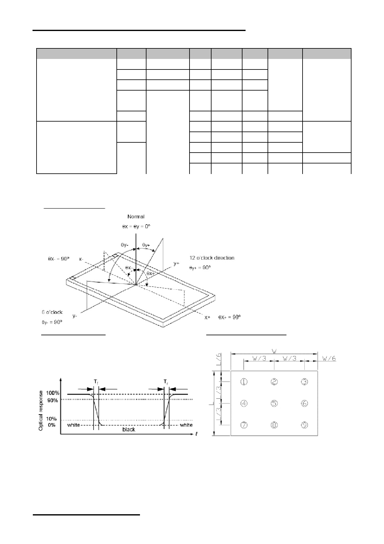
*1. Definition of Contrast Ratio
The contrast ratio could be calculate by the following expression:
Contrast Ratio (CR) = Luminanc with all pixels white / Luminance with all pixels black
*2 Definition of Viewing Angle
*3 Definition of response time
*4 Definition of Luminance Uniformity
Luminance uniformity (Lu)=
Min. Luminance form pt1~pt9 / Max Luminance form Pt1~pt9
*5. Measured with TFT and backlight only
URL: www.topwaydisplay.com
Document Name: LMT056DIDFWD-AEN-Manual-Rev0.2
Page: 28 of 29

TOPWAY
LCD Module User Manual
LMT056DIDFWD-AEN
9. Precautions of using LCD Modules
Please refer to "LCD-Module-Design-Handling-Precaution.pdf".
10. Appendix <Inspection items and criteria for appearance defect>
Bright/Dark Dots:
Defect Type
Specification
Major
Minor
Bright Dots
N≤ 2
●
Dark Dots
N≤ 3
●
Total Bright and Dark Dots
N≤ 4
●
Note: 1. The definition of dot: The size of a defective dot over 1/2 of whole dot is regarded as one defective dot.
2. Bright dot: Dots appear bright and unchanged in size in which LCD panel is displaying under black
pattern.
3. Dark dot: Dots appear dark and unchanged in size in which LCD panel is displaying under pure red,
green, blue pattern.
URL: www.topwaydisplay.com
Document Name: LMT056DIDFWD-AEN-Manual-Rev0.2
Page: 29 of 29