LMT080DIEFWU-AAN-2
LCD Module User Manual
Prepared by:
Checked by:
Approved by:
Wei
Date: 2017-07-25
Date:
Date:
Rev. Descriptions
Release Date
0.1
Preliminary release
2014-06-23
0.2
Update 6. AC Characteristics
2017-07-25
URL: www.topwaydisplay.com
Document Name: LMT080DIEFWU-AAN-2-Manual-Rev0.2
Page: 1 of 9

TOPWAY
LCD Module User Manual
LMT080DIEFWU-AAN-2
Table of Content
1. General Specification ............................................................................................................ 3
2. Block Diagram ........................................................................................................................ 3
3. Terminal Function .................................................................................................................. 4
3.1
LVDS Terminal (K2) ............................................................................................................................................... 4
3.2
Backlight Input Terminal (K3) ................................................................................................................................. 4
4. Absolute Maximum Ratings .................................................................................................. 4
5. Electrical Characteristics ...................................................................................................... 5
5.1
Driving TFT LCD Panel .......................................................................................................................................... 5
5.2
LED Backlight Circuit Characteristics ..................................................................................................................... 5
6. AC Characteristics ................................................................................................................. 6
6.1
AC Characteristics ( LVDS ) ................................................................................................................................. 6
6.2
AC Characteristics ( TFT ) .................................................................................................................................... 7
7. Optical Characteristics .......................................................................................................... 8
8. Precautions of using LCD Modules ...................................................................................... 9
URL: www.topwaydisplay.com
Document Name: LMT080DIEFWU-AAN-2-Manual-Rev0.2
Page: 2 of 9
TOPWAY
LCD Module User Manual
LMT080DIEFWU-AAN-2
1. General Specification
Signal Interface :
LVDS(VESA 24 bit)
Display Technology :
a-Si TFT active matrix
Display Mode :
Transmissive / Normal White
Screen Size(Diagonal) :
8.0”
Outline Dimension :
196.0 x 143.9 x12.2 (mm)
(see attached drawing for details)
Active Area :
162.0 x 121.5 (mm)
Number of dots :
800 x 600
Pixel Pitch :
0.2025 x 0.2025 (mm)
Pixel Configuration :
RGB Stripe
Backlight :
LEDs
Surface Treatment :
Anti-Glare Surface
Viewing Direction :
6 o’clock(Gray scale Inversion) (*1)
12 o’clock (*2)
Operating Temperature :
-20 ~ +70°C
Storage Temperature :
-30 ~ +80°C
Note:
*1. For saturated color display content (eg. pure-red, pure-green, pure-blue or pure-colors-combinations).
*2. For “ color scales ” display content.
*3. Color tone may slightly change by temperature and driving condition.
2. Block Diagram
BL_VDD, GND
BL_EN, BL_ADJ
LED Backlight
800(×3)×600 pixels
Source Driver
RX0+, RX0-, RX1+, RX1-
RX2+, RX2- ,RX3+, RX3-
RXC+, RXC-
LVDS Interface
Power Circuit
VCC_IN, GND
URL: www.topwaydisplay.com
Document Name: LMT080DIEFWU-AAN-2-Manual-Rev0.2
Page: 3 of 9
TOPWAY
LCD Module User Manual
LMT080DIEFWU-AAN-2
3. Terminal Function
3.1 LVDS Terminal (K2)
Pin No.
Pin Name
I/O
Descriptions
1
VCC_IN
Power
Positive Power Supply (3.3V)
2
VCC_IN
Power
Positive Power Supply (3.3V)
3
NC
-
NO connection
4
NC
-
NO connection
5
RX0-
Input
LVDS receiver negative signal channel 0
6
RX0+
Input
LVDS receiver positive signal channel 0
7
GND
Power
Power Supply GND (0V)
8
RX1-
Input
LVDS receiver negative signal channel 1
9
RX1+
Input
LVDS receiver positive signal channel 1
10
GND
Power
Power Supply GND (0V)
11
RX2-
Input
LVDS receiver negative signal channel 2
12
RX2+
Input
LVDS receiver positive signal channel 2
13
GND
Power
Power Supply GND (0V)
14
RXC-
Input
LVDS receiver negative signal clock
15
RXC+
Input
LVDS receiver positive signal clock
16
GND
Power
Power Supply GND (0V)
17
RX3-
Input
LVDS receiver negative signal channel 3
18
RX3+
Input
LVDS receiver positive signal channel 3
19
NC
-
NO connection
20
NC
-
NO connection
3.2 Backlight Input Terminal (K3)
Pin No.
Pin Name
I/O
Descriptions
1
GND
Power
Power Supply GND (0V)
2
GND
3
BL_ADJ
Input
Backlight dimming control (*1, *2)
PWM may be used to adjust the output brightness
4
BL_VDD
Power
Positive Power Supply(5V)
5
BL_VDD
Backlight driver enable (*1)
6
BL_EN
Input
BLON=Hi, Backlight Driving Booster enable
BLON=Lo, Backlight Driving Booster disable
Note:
*1. With built in pull up resistor, it could leave open
*2. Recommended PWM Freq. = 3kHz (active high)
4. Absolute Maximum Ratings
Items
Symbol
Min.
TYP. Max.
Unit
Condition
Power Supply Voltage
VCC_IN
-0.3
3.3
3.6
V
GND = 0V
Backlight Supply Voltage BL_VDD
-0.3
5.0
6.0
V
GND = 0V
Operating Temperature
T OP
-20
-
70
C
No Condensation
Storage Temperature
T ST
-30
-
80
C
No Condensation
Cautions:
Any Stresses exceeding the Absolute Maximum Ratings may cause substantial damage to the
device. Functional operation of this device at other conditions beyond those listed in the
specification is not implied and prolonged exposure to extreme conditions may affect device
reliability.
URL: www.topwaydisplay.com
Document Name: LMT080DIEFWU-AAN-2-Manual-Rev0.2
Page: 4 of 9
TOPWAY
LCD Module User Manual
LMT080DIEFWU-AAN-2
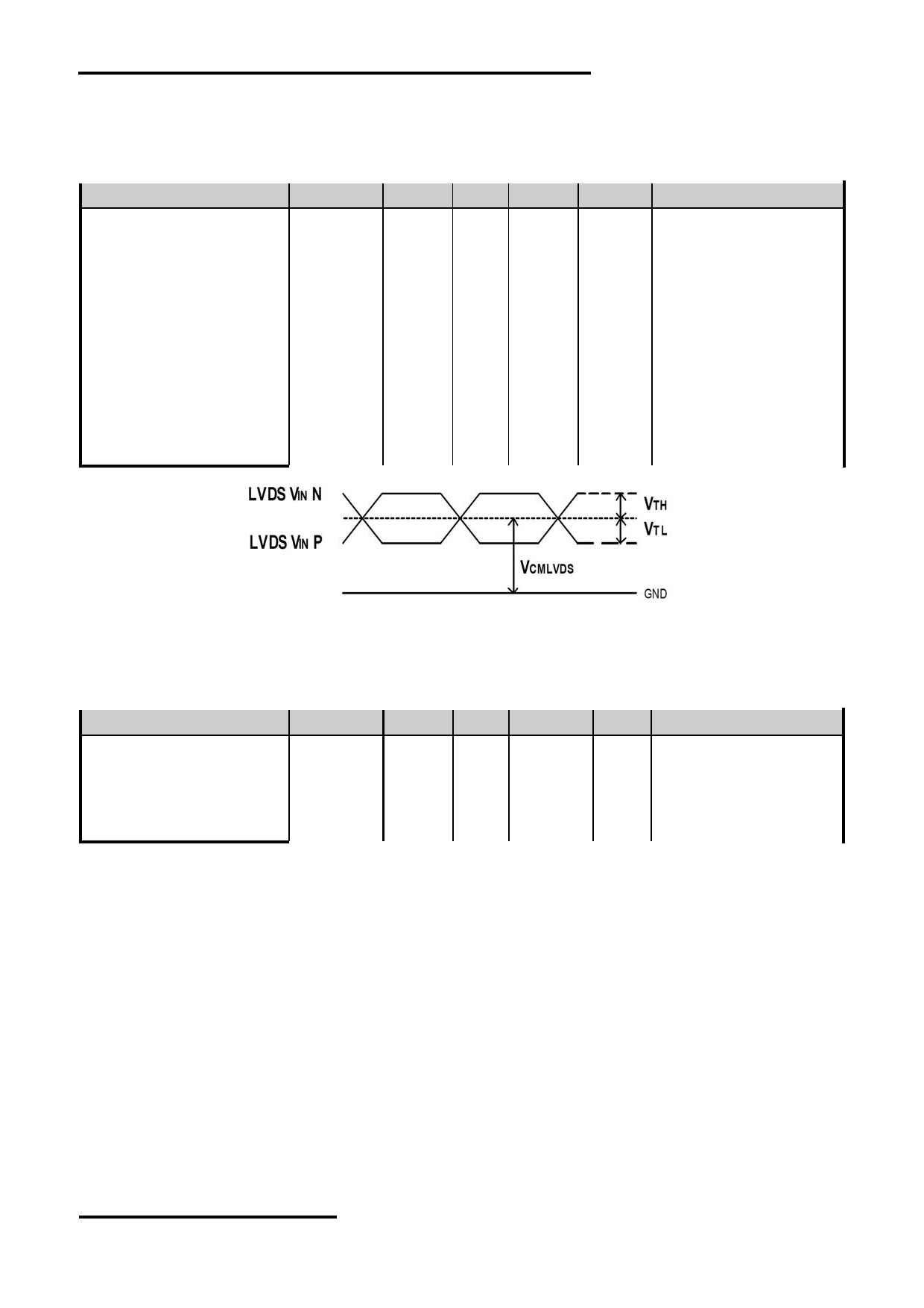
5. Electrical Characteristics
5.1 Driving TFT LCD Panel
GND=0V, VCC_IN=3.3V, T OP =25 C
Items
Symbol
MIN.
TYP. MAX.
Unit
Note
Supply Voltage
VCC_IN
3.0
3.3
3.5
V
Common Electrode
V CMLVDS
V
Note1
Driving Signal
-
1.2
-
Differential Input High
V TH
-
-
100
mV
Threshold
Differential Input Low
V TL
-100
-
-
mV
Threshold
Sync Frequency
FVD
-
60
70
Hz
VCC Power
I VCC_IN
-
150
-
mA
Consumption
LVDS DC timing diagram
Note1: The value may be different for different LCM.
5.2 LED Backlight Circuit Characteristics
GND=0V, T OP =25 C
Parameter
Symbol
MIN.
TYP.
MAX.
Unit
Note
Operating Voltage
BL_VDD
4.5
5.0
5.5
V
Input High Voltage
V IH
3.0
-
BL_VDD
V
BL_ADJ,BL_EN
Input Low Voltage
V IL
GND
-
0.3
V
BL_ADJ,BL_EN
Operating Current(*1)
I BL_VDD
-
412
-
mA BL_VDD
Cautions:
Exceeding the recommended driving current could cause substantial damage to the backlight and shorten its lifetime.
Note:
*1: BL_ADJ=Hi, BL_EN =Hi.
*2. Recommended BL_ADJ PWM Freq. is 3kHz (active high).
URL: www.topwaydisplay.com
Document Name: LMT080DIEFWU-AAN-2-Manual-Rev0.2
Page: 5 of 9

TOPWAY
LCD Module User Manual
LMT080DIEFWU-AAN-2
6. AC Characteristics
6.1 AC Characteristics ( LVDS )
VCC_IN =3.3V,GND=0V,Ta=25 ℃
Item
Symbol
MIN.
TYP.
MAX.
Unit
Condition
Input CLK period
t RI CLK
8.9
-
50
ns
Input Data Position 0
t RI 0
-0.3
-
+0.3
ns
( tRICLK = 8.9ns )
Input Data Position 1
t RI 1
t RI CLK/7-0.3
t RI CLK/7
t RI CLK/7+0.3
ns
(tRICLK = 8.9ns )
Input Data Position 2
t RI 2
2t RI CLK/7-0.3
2t RI CLK/7
2t RI CLK/7+0.3
ns
(tRICLK = 8.9ns )
Input Data Position 3
t RI 3
3t RI CLK/7-0.3
3t RI CLK/7
3t RI CLK/7+0.3
ns
(tRICLK = 8.9ns )
Input Data Position 4
t RI 4
4t RI CLK/7-0.3
4t RI CLK/7
4t RI CLK/7+0.3
ns
(tRICLK = 8.9ns )
Input Data Position 5
t RI 5
5t RI CLK/7-0.3
5t RI CLK/7
5t RI CLK/7+0.3
ns
(tRICLK = 8.9ns )
Input Data Position 6
t RI 6
6t RI CLK/7-0.3
6t RI CLK/7
6t RI CLK/7+0.3
ns
(tRICLK = 8.9ns )
URL: www.topwaydisplay.com
Document Name: LMT080DIEFWU-AAN-2-Manual-Rev0.2
Page: 6 of 9
TOPWAY
LCD Module User Manual
LMT080DIEFWU-AAN-2
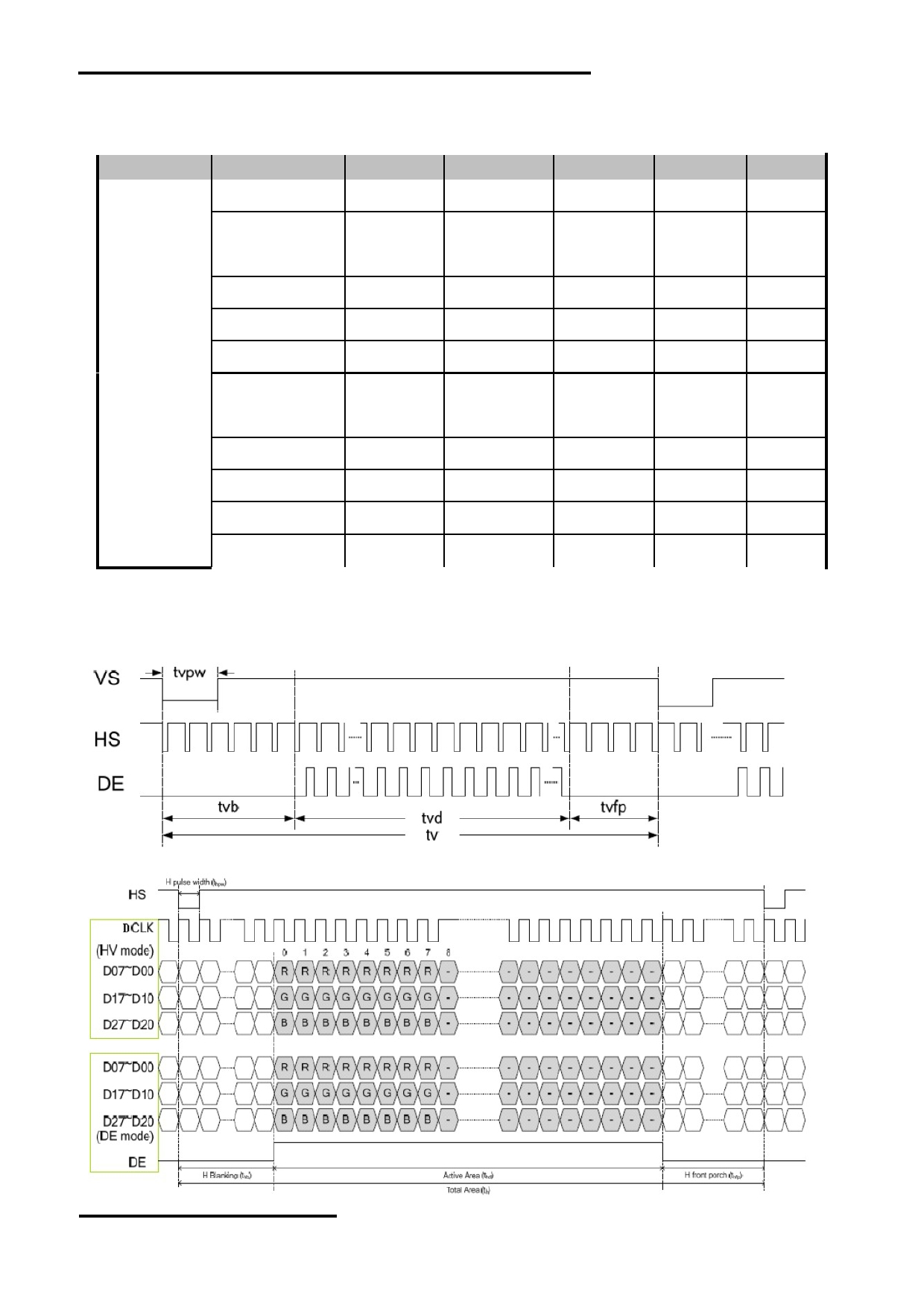
6.2 AC Characteristics ( TFT )
Parameter
Symbol
Min
Typ
Max
Unit
Remark
F clk
34.5
39.6
50.4
MHz
DCLK
t clk
-
25.3
-
ns
t h
900
1000
1200
DCLK
t hd
-
800
-
DCLK
t hpw
1
-
40
DCLK
HSD
t hb
-
88
-
DCLK
t hfp
12
112
312
DCLK
t v
640
660
700
th
t vd
-
600
-
th
t vpw
1
-
20
th
VSD
t vb
-
39
-
th
t vfp
1
21
61
th
Note: DE timing refer to HSD, VSD input timing.
Vertical input timing Diagram
Horizontal input timing Diagram
URL: www.topwaydisplay.com
Document Name: LMT080DIEFWU-AAN-2-Manual-Rev0.2
Page: 7 of 9
TOPWAY
LCD Module User Manual
LMT080DIEFWU-AAN-2
7. Optical Characteristics
Test Conditions:
1. I F = 180mA, V F =9.6V, and the ambient temperature is 25 ℃ .
2. The test systems refer to Note 1 and Note 2.
VCC_IN =3.3V,GND=0V,Ta=25 ℃
Item
Symbol
Condition
MIN.
TYP.
MAX.
UNIT
Note.
θ L
9 o’clock
60
70
-
Viewing angle
θ R
3 o’clock
60
70
-
(CR ≥ 10)
degree
Note 2
θ T
12 o’clock
50
60
-
θ B
6 o’clock
60
70
-
T f
ms
Response Time
25 ℃
-
25
30
Note 1
T r
ms
Note 4
Contrast ratio
CR
θ=0 o
600
800
-
-
Note 1,3
X
0.253
0.303
0.353
White
Y
0.257
0.307
0.357
X
0.525
0.575
0.625
Red
Color
Y
Backlight 0.296 0.346
0.396
Note 1
chromaticlty
X
is on
0.298
0.348
0.398
Note 5
Green
Y
0.527
0.577
0.627
X
0.101
0.151
0.201
Blue
Y
0.031
0.081
0.131
Luminance
L
-
250
-
cd/m 2
Note 1,6
Luminance uniformity
Y U
70
75
-
%
Note 1,7
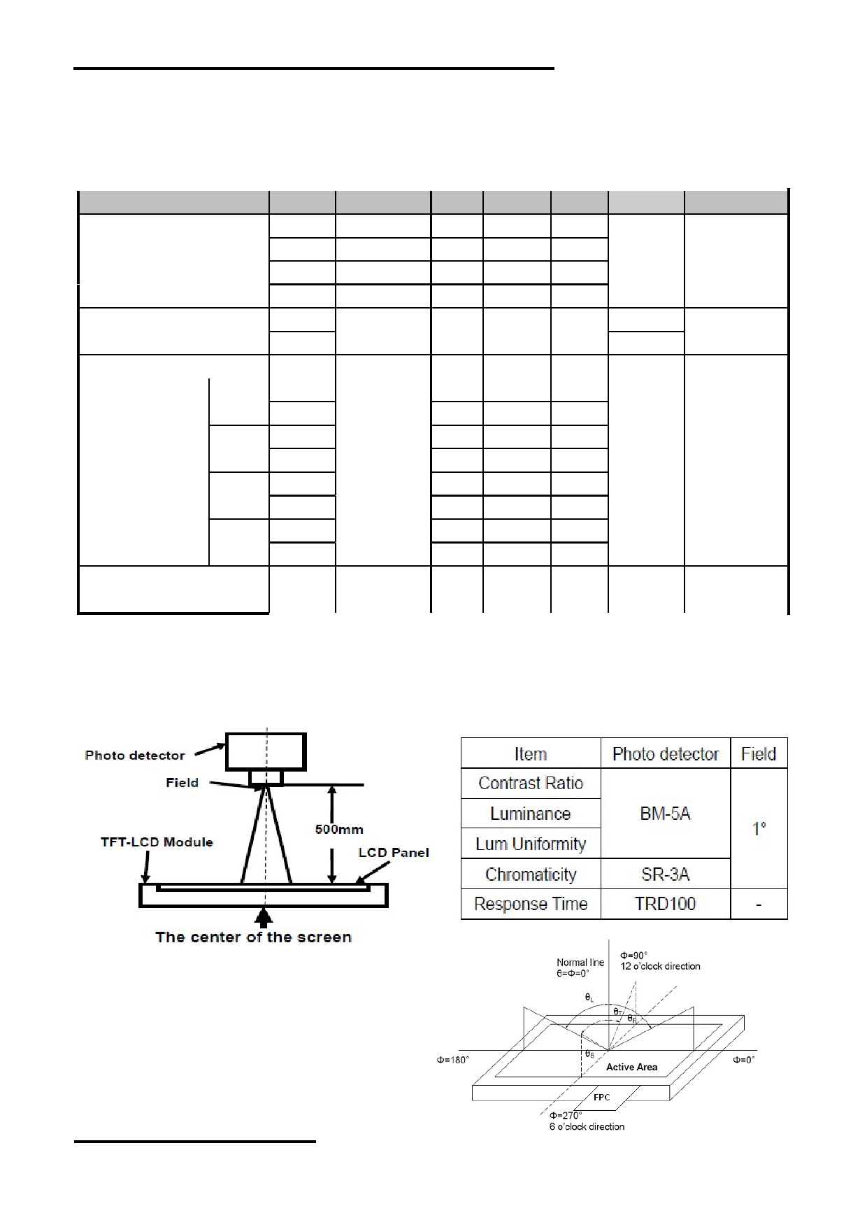
Note 1: Definition of optical measurement system.
The optical characteristics should be measured in dark room. After 5 Minutes operation, the optical
properties are measured at the center point of the LCD screen. All input terminals LCD panel must
be ground when measuring the center area of the panel.
Note 2: Definition of viewing angle range
URL: www.topwaydisplay.com
Document Name: LMT080DIEFWU-AAN-2-Manual-Rev0.2
Page: 8 of 9

TOPWAY
LCD Module User Manual
LMT080DIEFWU-AAN-2
Note 3: Definition of contrast ratio
Note 4: Definition of Response time
The response time is defined as the LCD optical switching time interval between “ White ” state
and
“ Black ” state. Rise time (T ON ) is the time between photo detector output intensity changed from
90% to 10%. And fall time (T OFF ) is the time between photo detector output intensity changed from
10% to 90%.
Note 5: Definition of color chromaticity (CIE1931)
Color coordinates measured at center point of LCD.
Note 6: Definition of Luminance Uniformity
Active area is divided into 9 measuring areas (Refer Fig. 2). Every measuring point is placed at the
center of each measuring area.
Luminance Uniformity (U) = Lmin/ Lmax
L-------Active area length W----- Active area width
Lmax: The measured Maximum luminance of all measurement position.
Lmin: The measured Minimum luminance of all measurement position.
Note 7: Definition of Luminance:
Measure the luminance of white state at center point.
8. Precautions of using LCD Modules
Please refer to "LCD-Module-Design-Handling-Precaution.pdf".
URL: www.topwaydisplay.com
Document Name: LMT080DIEFWU-AAN-2-Manual-Rev0.2
Page: 9 of 9