LMT101DNLFWD-NND10
LCD Module User Manual
Prepared by:
Checked by:
Approved by:
Pengzhen
Date: 2026-07-01
Date:
Date:
Rev. Descriptions
Edit
Release Date
0.1
Preliminary
Pengzhen
2026-07-01
URL: www.topwaydisplay.com
Document Name: LMT101DNLFWD-NND10-Manual-Rev0.1.doc
Page: 1 of 18

TOPWAY
LCD Module User Manual
LMT101DNLFWD-NND10
Table of Content
1. General Specification........................................................................................................... 3
2. Block Diagram......................................................................................................................3
3. Terminal Function.................................................................................................................4
3.1 CN1 TFT Input Terminal(JAE FI-SE20P-HFE-E3000or equivalent)...............................4
3.2 CN2 Backlight Terminal (JAE FI-S6P-HFE-E1500 or equivalent).................................. 4
3.3 CN3 CTP Terminal (MOLEX 53261-0871 Or Equivalent).............................................. 4
4. Absolute Maximum Ratings..................................................................................................5
5. Electrical Characteristics......................................................................................................6
5.1 DC Characteristics for Panel Driving..............................................................................6
5.2 DC Characteristics for Backlight Driving........................................................................ 6
5.3 DC Characteristics for CTP Driving................................................................................6
5.4 Recommended Power ON/OFF Sequence....................................................................7
6. Timing Characteristics..........................................................................................................8
6.1 AC characteristics.......................................................................................................... 8
6.2 LVDS DC characteristics................................................................................................9
6.3 Data Input timing Parameter Setting............................................................................10
6.4 Data Input Format........................................................................................................ 11
7. Optical Characteristics....................................................................................................... 12
8. LCD Module Design and Handling Precautions................................................................. 14
9. CTP Mounting Instructions.................................................................................................15
10. TFT QA Standard............................................................................................................. 16
10.1 INSPECTION CONDITION 检验条件 ..................................................................... 16
10.2 Display Pattern 显示缺陷 .........................................................................................16
10.3 Exterior 外观缺陷 .....................................................................................................17
10.4 Quality Level and Sampling 抽样方法 ......................................................................18
URL: www.topwaydisplay.com
Document Name: LMT101DNLFWD-NND10-Manual-Rev0.1.doc
Page: 2 of 18
TOPWAY
LCD Module User Manual
LMT101DNLFWD-NND10
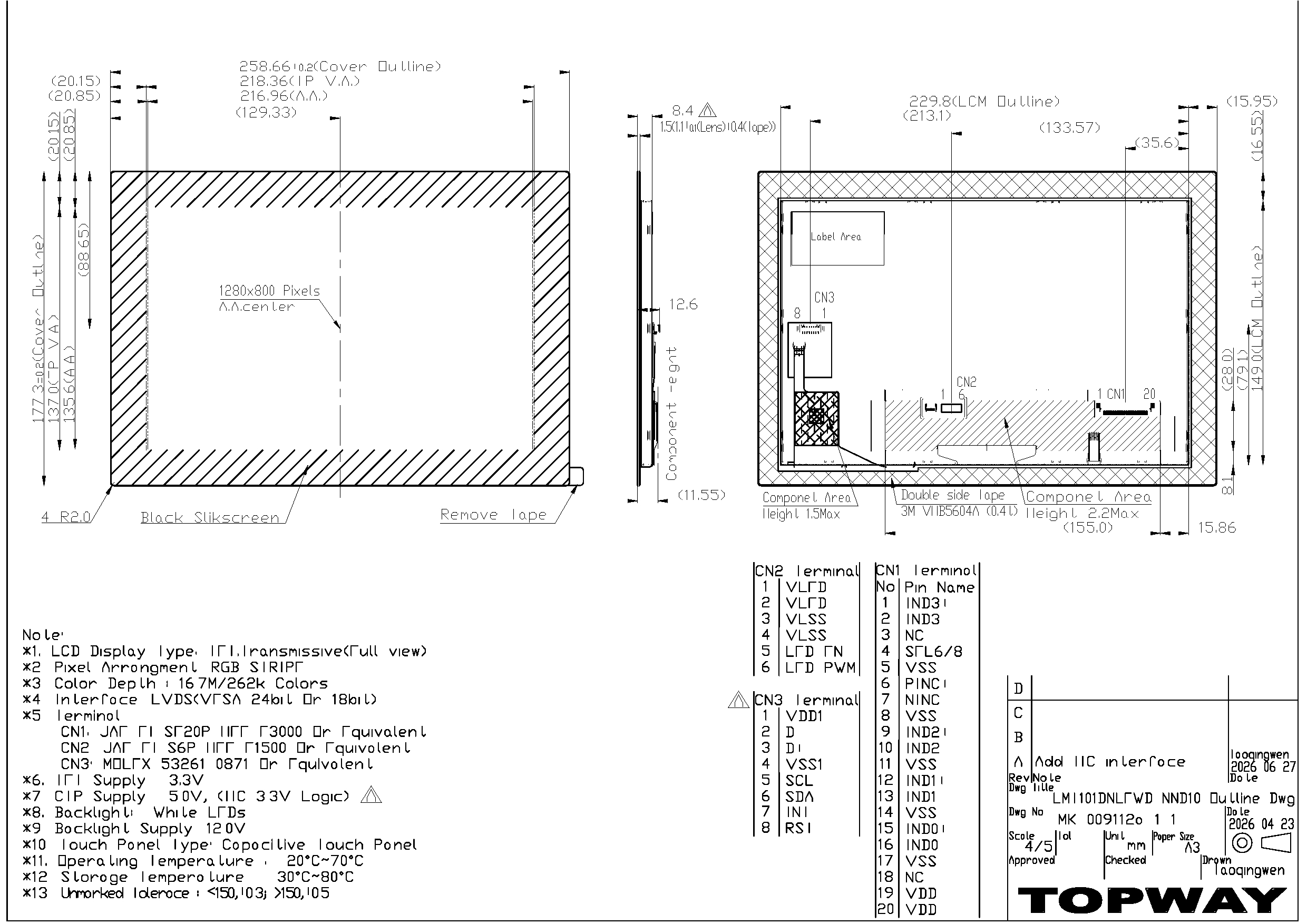
1. General Specification
Screen Size(Diagonal) :
10.1”
Active Area :
216.96x 135.60(mm)
Number of dots :
1280(RGB) x800
Pixel Pitch :
0.1695 x 0.1695(mm)
Color Depth:
16.7M
Display Technology :
a-Si
Signal Interface:
LVDS 18bit/24bit (VESA)
Display Mode:
Normal Black, Transmissive
Outline Dimension:
258.66x177.30x12.60(mm)
(see outline drawing for details)
Pixel Configuration:
R.G.B. Vertical Stripe
Viewing Direction :
F ull
Touch Panel Type :
Capacitive Touch Panel
Backlight :
White LED s
Operating Temperature :
-20 ~ +70°C
Storage Temperature :
-30 ~ +80°C
Note:
*1. Color tone may slightly change by temperature and driving condition.
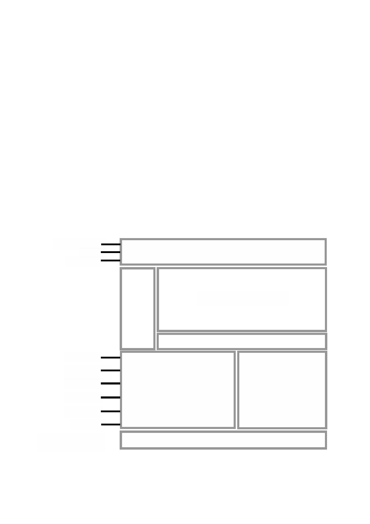
2. Block Diagram
SDA,SCL,RST,INT
D+,D-
Touch Panel
VDD1,VSS1
1280(RGB ) x 800 pixels
Source Driver
IND3+,IND3-
PINC+,NINC-
IND2+,IND2-
LVDS Interface
Power Circuit
IND1+,IND1-
IND0+,IND0-
VDD,VSS
VLED,VLSS
LED_EN,LED_PWM
Backlight Circuit
URL: www.topwaydisplay.com
Document Name: LMT101DNLFWD-NND10-Manual-Rev0.1.doc
Page: 3 of 18
TOPWAY
LCD Module User Manual
LMT101DNLFWD-NND10
3. Terminal Function
3.1
CN1 TFT Input Terminal(JAE FI-SE20P-HFE-E3000or equivalent)
NO Symbol
I/O Description
Comment
1
IND3+
I
Positive LVDS Differential data input(3)
2
IND3-
I
Negative LVDS Differential data input(3)
3
NC
N
No connection
4
SEL6/8
I
6bit/8bit mode select
H : 6-bit mode
L or Open : 8-bit mode
5
VSS
P
Power Ground
6
PINC+
I
Positive LVDS Differential clock input
7
NINC-
I
Negative LVDS Differential clock input
8
VSS
P
Power Ground
9
IND2+
I
Positive LVDS Differential data input(2)
10
IND2-
I
Negative LVDS Differential data input(2)
11
VSS
P
Power Ground
12
IND1+
I
Positive LVDS Differential data input(1)
13
IND1-
I
Negative LVDS Differential data input(1)
14
VSS
P
Power Ground
15
IND0+
I
Positive LVDS Differential data input(0)
16
IND0-
I
Negative LVDS Differential data input(0)
17
VSS
P
Power Ground
18
NC
N
No Connection
19
VDD
P
Power Supply(3.3V)
20
VDD
P
Power Supply(3.3V)
Note1: I/O definition: I---Input, O---Output, P---Power/Ground, N---No connection
Note2: All of the GND pins should be connected to the system ground.
3.2
CN2 Backlight Terminal (JAE FI-S6P-HFE-E1500 or equivalent)
NO Symbol
I/O Description
Comment
1
VLED
P
Backlight power supply(12V)
2
VLED
P
Backlight power supply(12V)
3
VLSS
P
VLED Ground
4
VLSS
P
VLED Ground
5
LED_EN
I
Backlight on/off control
6
LED_PWM I
Backlight dimming control
Note1: I/O definition: I---Input, O---Output, P---Power/Ground, N---No connection
3.3
CN3 CTP Terminal (MOLEX 53261-0871 Or Equivalent)
NO Symbol
I/O Description
Comment
1
VDD1
P
Power for CTP(5V)
2
D-
I/O USB data- pin
3
D+
I/O USB data+ pin
4
VSS1
P
Power Ground
5
SCL
I
Clock Signal
6
SDA
I
Data Signal
7
INT
O
Interrupt Signal, Falling Edge Effective
8
RST
I
Reset Signal
Note1: I/O definition: I---Input, O---Output, P---Power/Ground, N---No connection
Note2: Capacitor screen can support USB interface and IIC interface, but it cannot be used at the same time.
URL: www.topwaydisplay.com
Document Name: LMT101DNLFWD-NND10-Manual-Rev0.1.doc
Page: 4 of 18
TOPWAY
LCD Module User Manual
LMT101DNLFWD-NND10
4. Absolute Maximum Ratings
Items
Symbol
Min.
Max. Unit Condition
Power Voltage
VDD
-0.3
3.4
V
Input voltage for Display signals
VDDRX
-0.3
3.4
V
Note1
Power supply voltage for Backlight
VLED
-0.3
12.5
V
Input voltage for Backlight signals
LED_EN
-0.3
12.5
V
LED_PWM
-0.3
4
V
Input voltage for CTP
VDD1
-0.3
5.5
V
Operating Temperature
Top
-20
70
℃
Storage Temperature
Tst
-30
80
℃
-
≤ 95
%
Ta≤40 ℃
-
≤ 85
%
40 ℃ < Ta≤50 ℃
Relative Humidity
-
%
Note2
RH
≤ 55
50 ℃ < Ta≤60 ℃
-
≤ 36
%
60 ℃ < Ta≤70 ℃
-
≤ 24
%
70 ℃ < Ta≤80 ℃
Absolute Humidity
AH
-
≤ 70 g/m³ Ta > 70 ℃
Note1: VDDRX include IND0-/+ 、 IND1-/+ 、 IND2-/+ 、 IND3-/+ 、 PINC 、 NINC
Note2: Ta means the ambient temperature. It is necessary to limit the relative humidity to the specified
temperature range. Condensation on the module is not allowed.
Note3: The absolute maximum rating values of this product are not allowed to be exceeded at any times. A
module should be used with any of the absolute maximum ratings exceeded, the characteristics of the
module may not be recovered, or in an extreme condition, the module may be permanently destroyed
URL: www.topwaydisplay.com
Document Name: LMT101DNLFWD-NND10-Manual-Rev0.1.doc
Page: 5 of 18
TOPWAY
LCD Module User Manual
LMT101DNLFWD-NND10
5. Electrical Characteristics
5.1
DC Characteristics for Panel Driving
VCC=3.3V, GND=0V,T op =25°C
Items
Symbol
MIN.
TYP.
MAX.
Unit Remark
Supply Voltage
VCC
3.2
3.3
3.4
V
Input Signal Voltage Low Level
VIL
GND
-
0.2xVDD
V
High Level
VIH
0.8xVDD
-
VDD
V
Output Signal
Low Level
VOL
GND
-
0.2xVDD
V
Voltage
High Level
VOH 0.8xVDD
-
VDD
V
Power Consumption 60Hz
P
-
TBD
-
mW
White
patten
Note: All display qualities are guaranteed only under the TYP value.
5.2
DC Characteristics for Backlight Driving
T op =25°C
Items
Symbol
MIN.
TYP.
MAX.
Unit Remark
Backlight power supply voltage
VLED
11.5
12
12.5
V
Backlight Current
I VLED
-
600
-
mA 36 LEDs
Backlight Power Consumption
WBL
-
7200
-
mW (6 LED
PWM frequency
Fpwm
100
-
50K
Hz Parallel,6
PWM duty
D
5
-
100
% LED Serial)
LED life time
-
-
50000
-
Hrs
Note1: Optical performance should be evaluated at Ta=25 ℃ only.
Note2: If LED is driven by high current, high ambient temperature & humidity condition,The life time of
LED will be reduced.
Note3: Operating life means brightness goes down to 50% of initial brightness. Typical operating life
time is estimated data.
5.3
DC Characteristics for CTP Driving
T op =25°C
Items
Symbol
MIN.
TYP.
MAX.
Unit Remark
Power supply voltage
VDD1
4.7
5.0
5.3
V
Power supply current
I_VDD1
-
100
-
mA Note1
Note1: All current measurement is average current at Operating mode.
URL: www.topwaydisplay.com
Document Name: LMT101DNLFWD-NND10-Manual-Rev0.1.doc
Page: 6 of 18
TOPWAY
LCD Module User Manual
LMT101DNLFWD-NND10
5.4
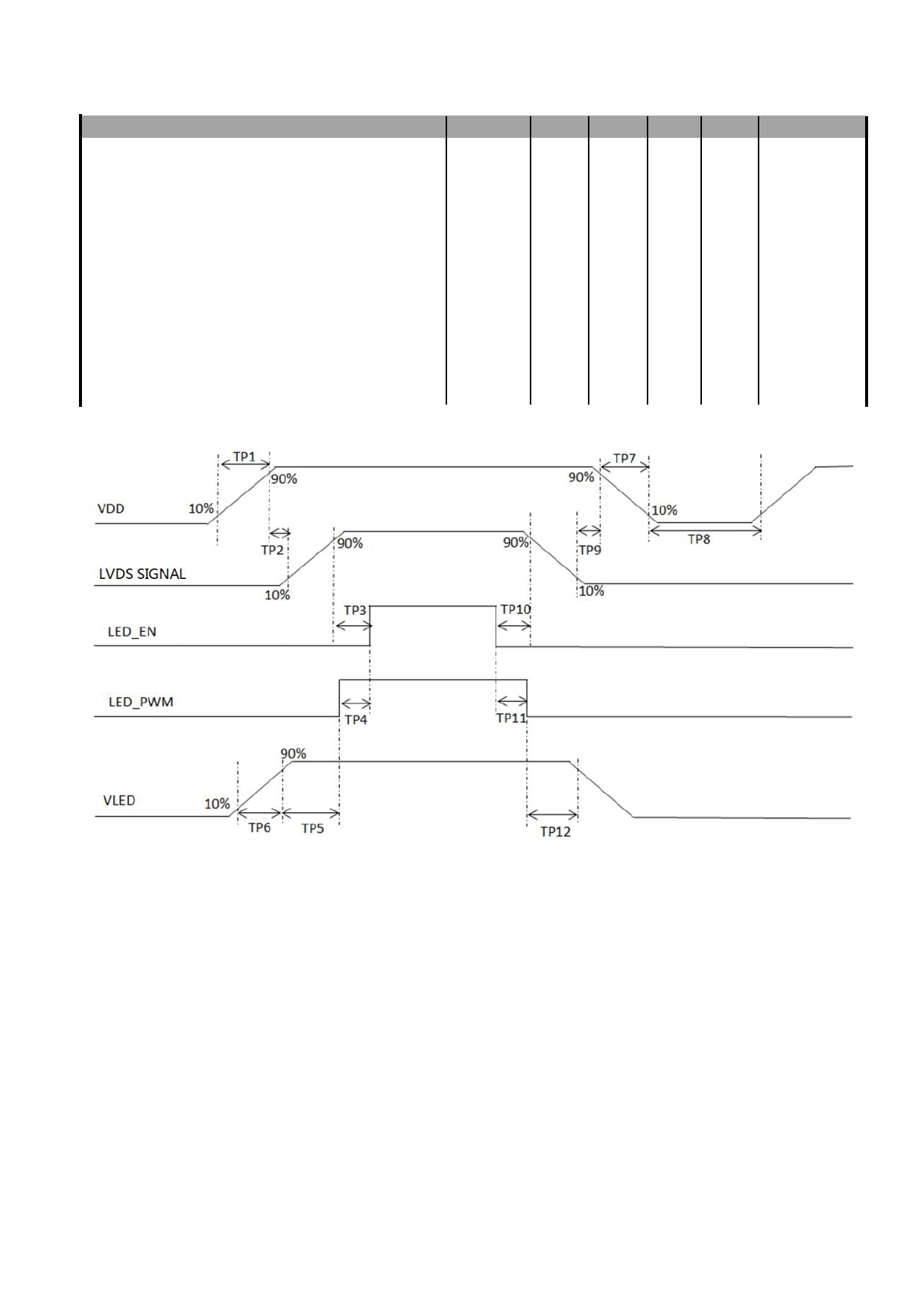
Recommended Power ON/OFF Sequence
Items
Symbol Min Typ Max Unit
Remark
VDD on to VDD stable
Tp1
0.5
-
10
ms
VDD stable to signal on
Tp2
200
-
-
ms
Signal on to LED_EN on
Tp3
200
-
-
ms
LED_PWM on to LED_EN on
Tp4
0
-
200 ms
VLED to LED_ PWM on
Tp5
10
-
-
ms
VLED on to VLED stable
Tp6
0.5
-
10
ms
VDD off time
Tp7
0
-
10
ms
VDD off to next VDD on
Tp8
1000
-
-
ms
Signal off before VDD off
Tp9
0
-
50
ms
LED_EN off before signal off
Tp10
200
-
-
ms
LED_EN off before LED_PWM off
Tp11
0
-
200 ms
LED_PWM off before VLED off
Tp12
10
-
-
ms
Note1: It is advised that backlight turned on later than display stabled.
Note2: The low level of these signals and analog powers are GND level.
Note3: All of the power and signals should be kept at GND level before power on. If there are residual voltages
on them, the LCD might not work properly.
URL: www.topwaydisplay.com
Document Name: LMT101DNLFWD-NND10-Manual-Rev0.1.doc
Page: 7 of 18
TOPWAY
LCD Module User Manual
LMT101DNLFWD-NND10
6. Timing Characteristics
6.1
AC characteristics
Parameter
Symbol
Min
Typ
Max
Unit
Remark
1 data bit time
UI
-
1/7
-
R xTCLK
Clock high time
T LVCH
-
4
-
UI
Clock low time
T LVCL
-
3
-
UI
Position 1
T POS1
-0.25
0
0.25
UI
Position 2
T POS2
0.75
-
1.25
UI
Position 3
T POS3
0.75
1
1.25
UI
Position 4
T POS4
1.75
-
2.25
UI
Position 5
T POS5
1.75
2
2.25
UI
Position 6
T POS6
2.75
-
3.25
UI
Position 7
T POS7
2.75
3
3.25
UI
Position 8
T POS8
3.75
-
4.25
UI
Position 9
T POS9
3.75
4
4.25
UI
Position 10
T POS10
4.75
-
5.25
UI
Position 11
T POS11
4.75
5
5.25
UI
Position 12
T POS12
5.75
-
6.25
UI
Position 13
T POS13
5.75
6
6.25
UI
Position 14
T POS14
6.75
-
7.25
UI
Input eye width
T EYEW
0.5
-
-
UI
Input eye border
T EX
-
-
0.25
UI
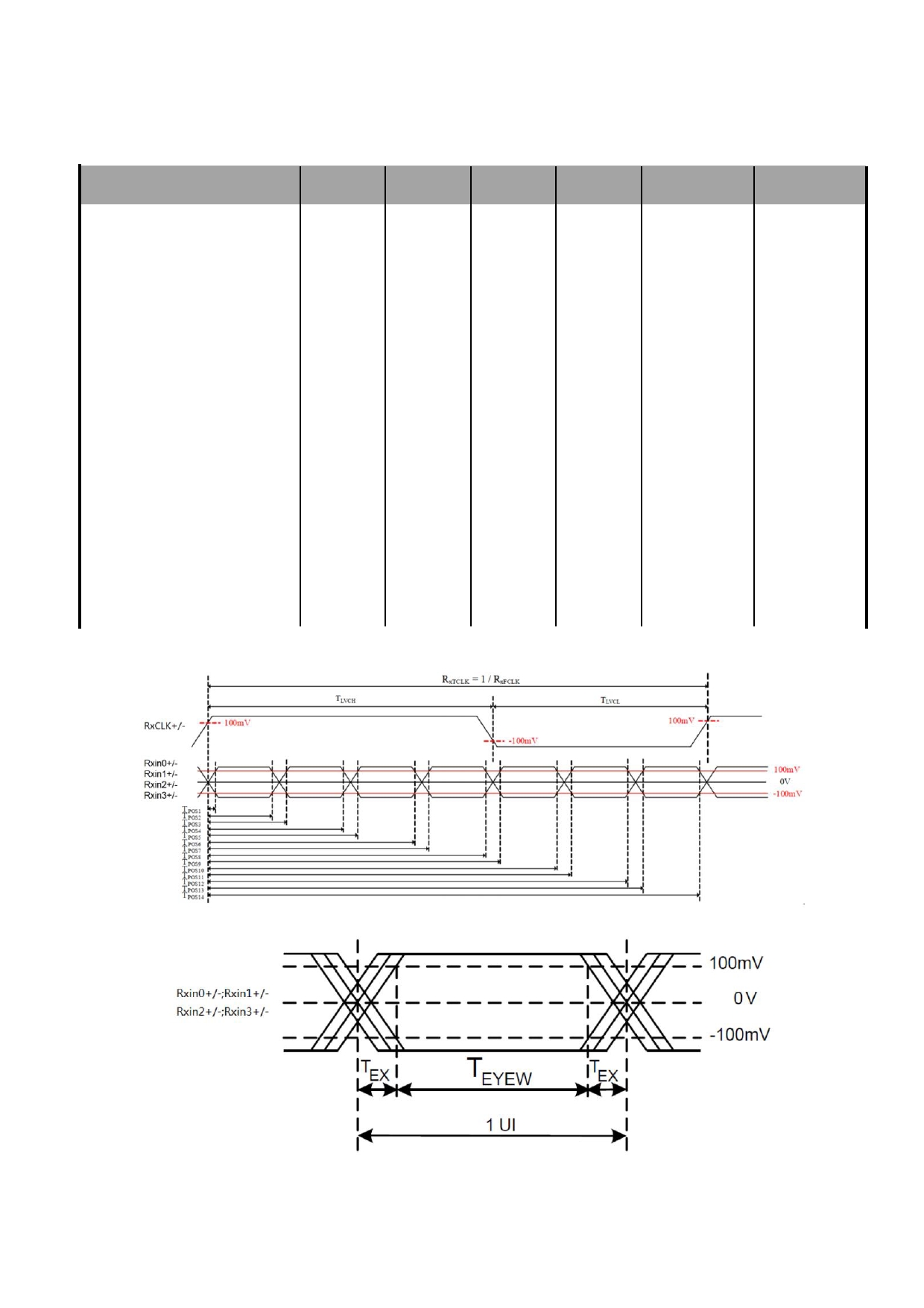
Input Setup Timing Parameters Requirement
Clock and Data Input Timing Diagram
URL: www.topwaydisplay.com
Document Name: LMT101DNLFWD-NND10-Manual-Rev0.1.doc
Page: 8 of 18
TOPWAY
LCD Module User Manual
LMT101DNLFWD-NND10
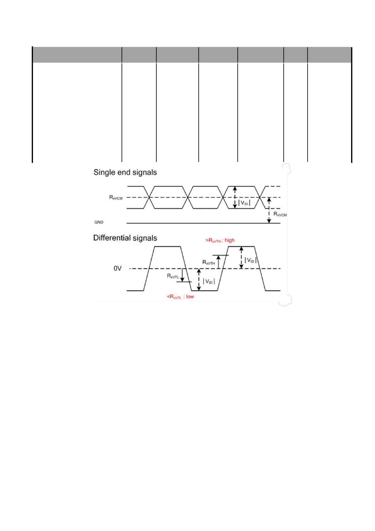
6.2
LVDS DC characteristics
Parameter
Symbol
Min
Typ
Max
Unit
Remark
Differential input high
Threshold voltage
R XVTH
-
-
0.1
V
Differential input Low
Threshold voltage
R XVTL
-0.1
-
-
V
Input voltage
range(single-end)
R XVIN
0
-
VDD-1.0
V
VDD=3.3V
Differential input
common Mode voltage
R XVCM
0.6
1.2
2.4-|VID|/2
V
Differential input voltage
|V ID |
> R XVT
0.4
0.6
V
Differential input
leakage current
RVxliz
-10
-
10
uA
LVDS DC characteristics
URL: www.topwaydisplay.com
Document Name: LMT101DNLFWD-NND10-Manual-Rev0.1.doc
Page: 9 of 18
TOPWAY
LCD Module User Manual
LMT101DNLFWD-NND10
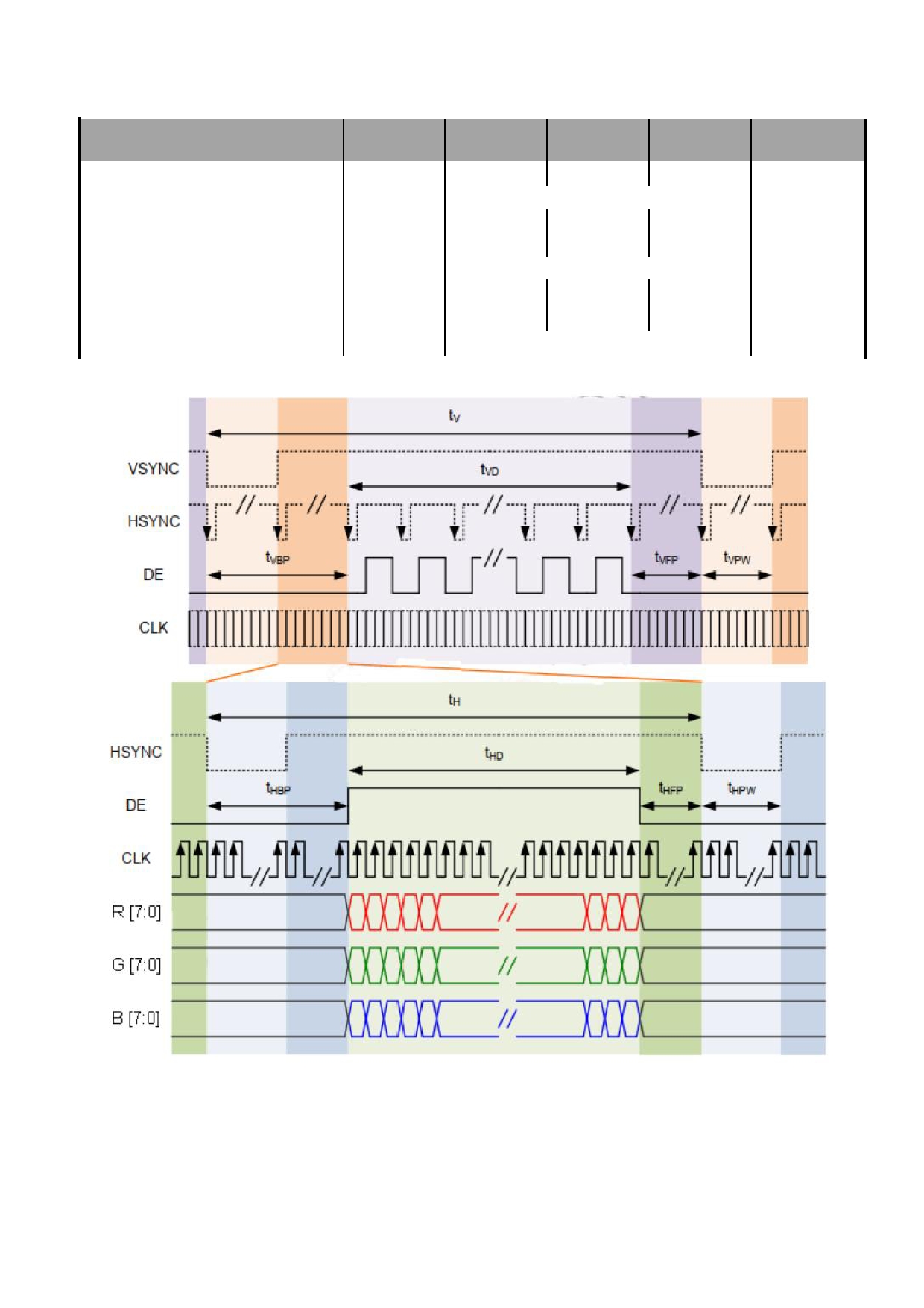
6.3 Data Input timing Parameter Setting
Parameter
Symbol
Min
Typ
Max
Unit
CLK frequency
tclk
68.1
69.8
71.4
MHz
Horizontal display area
thd
1280
tclk
Horizontal Blanking time
thbt
79
104
129
tclk
HSYNC period
th
1359
1384
1409
tclk
Vertical display area
tvd
800
th
Vertical Blanking time
tvbt
35
40
45
th
VSD period
tv
835
840
845
th
Frame rate
FR
60
Hz
Data Input timing Parameter Setting
URL: www.topwaydisplay.com
Document Name: LMT101DNLFWD-NND10-Manual-Rev0.1.doc
Page: 10 of 18
TOPWAY
LCD Module User Manual
LMT101DNLFWD-NND10
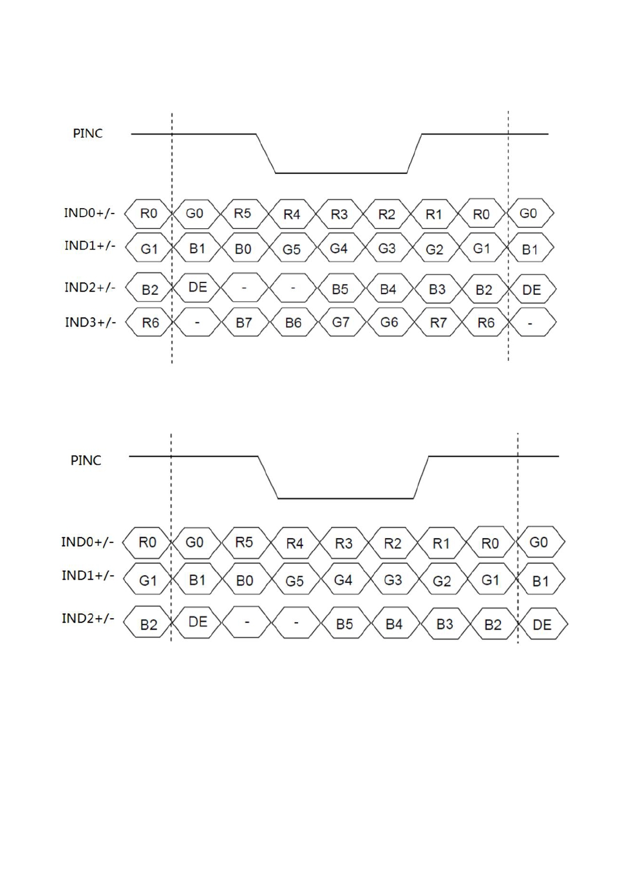
6.4 Data Input Format
8-bit mode data input
8-bit Data Input Format
6-bit mode data input
6-bit Data Input Format
URL: www.topwaydisplay.com
Document Name: LMT101DNLFWD-NND10-Manual-Rev0.1.doc
Page: 11 of 18
TOPWAY
LCD Module User Manual
LMT101DNLFWD-NND10
7. Optical Characteristics
Item
Symbol Condition MIN TYP MAX
Unit
Remark
θ T
80
89
-
θ B
80
89
-
Viewing angle
CR ≥ 10
degree
Note2,3
θ L
80
89
-
θ R
80
89
-
Contrast Ratio
CR
θ=0 o
900
1200
-
Note3
T ON
Response Time
25 ℃
35
45
ms
Note4
T OFF
x
0.252
0.302
0.352
White
-
y
0.277
0.327
0.377
x
0.532
0.582
0.632
Red
-
y
Backlight is
0.274
0.324
0.374
Chromaticity
on
Note1,5
x
0.300
0.350
0.400
Green
-
y
0.532
0.582
0.632
x
0.104
0.154
0.204
Blue
-
y
0.044
0.094
0.144
Uniformity
U
75
80
-
%
Note6
NTSC
-
67
72
-
%
Note5
Luminance
L
700
850
-
cd/m 2
Note7
Test Conditions:
1. The ambient temperature is 25 ℃ .
2. The test systems refer to Note1 and Note2.
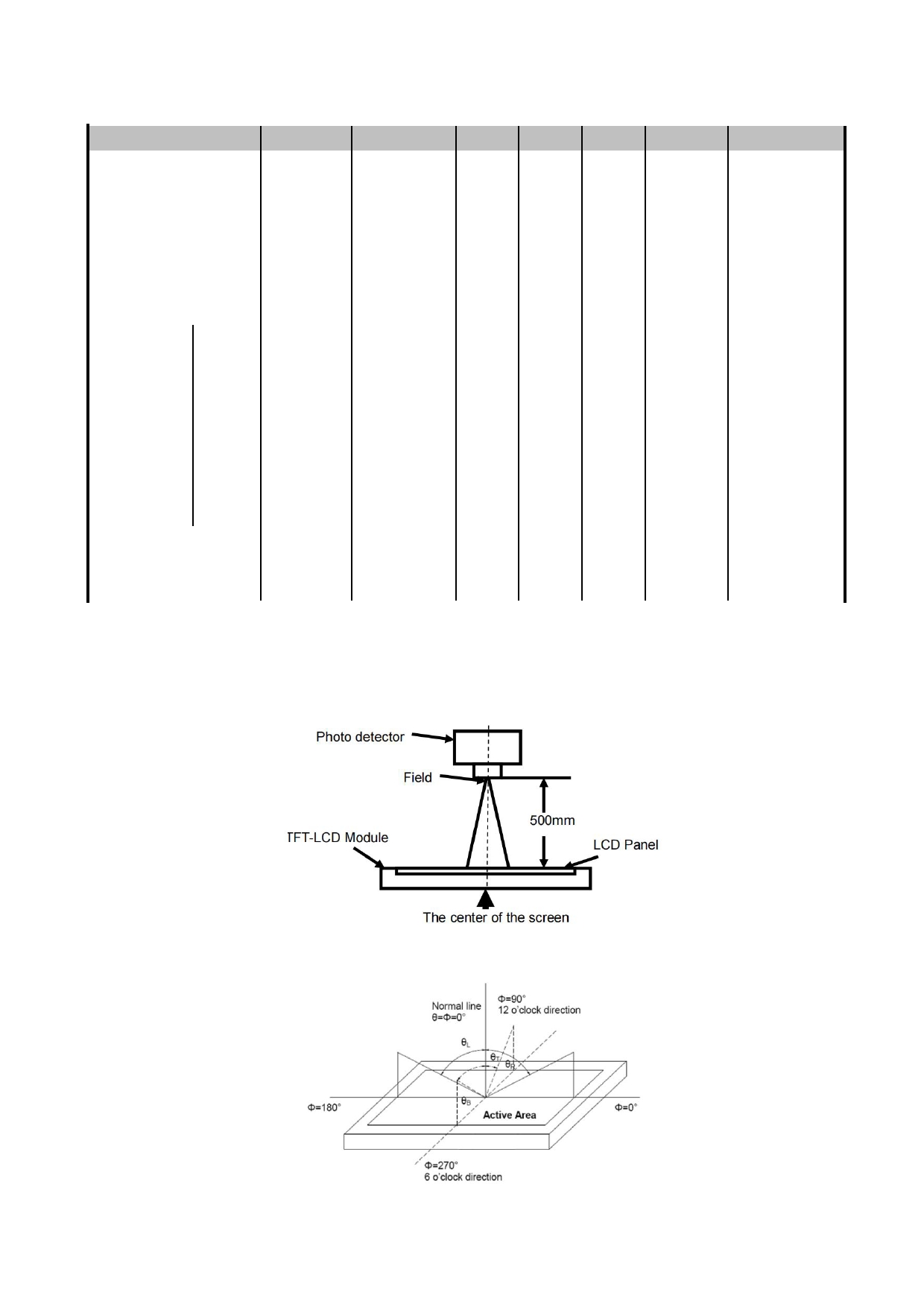
Note1: Definition of optical measurement system.
The optical characteristics should be measured in dark room. After 5 Minutes operation, the optical
characteristics are measured at the center point of the LCD screen.
Measurement Set Up
Note2: Definition of viewing angle range and measurement system. Viewing angle is measured at the center
point of the LCD.
Measurement viewing angle
URL: www.topwaydisplay.com
Document Name: LMT101DNLFWD-NND10-Manual-Rev0.1.doc
Page: 12 of 18
TOPWAY
LCD Module User Manual
LMT101DNLFWD-NND10
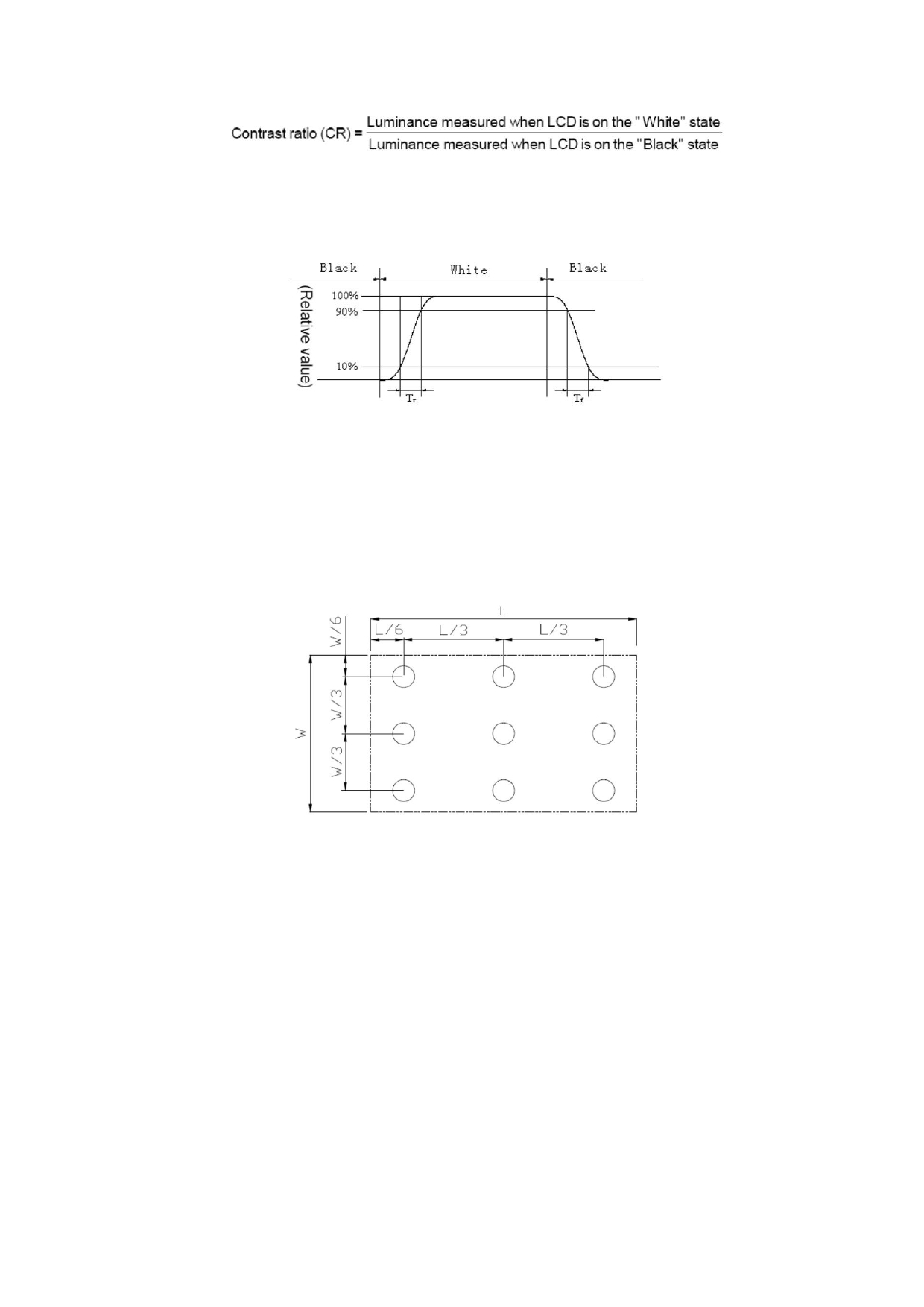
Note3: Definition of contrast ratio
Note4: Definition of Response time
For SFT LCM, the response time is defined as the LCD optical switching time interval between
“ White ” state and “ Black ” state. Rise time (Tr) is the time between photo detector output
intensity changed from 10% to 90%. And fall time (Tf) is the time between photo detector output
intensity changed from 90% to 10%.
Response Time Testing(SFT)
Note5: Definition of color chromaticity (CIE1931)
Color coordinates measured at center point of LCD.
Note6: Definition of Luminance Uniformity
Active area is divided into 9 measuring areas (Refer Fig.5). Every measuring point is placed at the
center of each measuring area.
Luminance Uniformity (U) = Lmin/ Lmax
Lmax: The measured Maximum luminance of all measurement position.
Lmin: The measured Minimum luminance of all measurement position.
L-------Active area length; W----- Active area width
Luminance Uniformity Measurement Locations(9 points)
Note7: Definition of Luminance:
Measure the luminance of white state at center point .
URL: www.topwaydisplay.com
Document Name: LMT101DNLFWD-NND10-Manual-Rev0.1.doc
Page: 13 of 18

TOPWAY
LCD Module User Manual
LMT101DNLFWD-NND10
8. LCD Module Design and
8. 液晶显示模块设计和使用须知
Handling Precautions
- Please ensure V0, VCOM is adjustable, to enable LCD module get - 请注意 V0, VCOM 的设定 , 以确保液晶显示模块在不同
the best contrast ratio under different temperatures, view angles
的使用温度下以及在不同的视角和位置观察模块显
and positions.
示,均能达到最佳对比度,请务必将应用电路上设置
为对比度可调。
- Normally display quality should be judged under the best contrast - 请注意液晶显示模块的显示品质判定是指在正常对比
ratio within viewable area. Unexpected display pattern may come
度下以及视窗 (V.A) 范围内进行的,非正常对比度下液
out under abnormal contrast ratio.
晶可能会出现非预期的显示不良,应注意区分。
- Never operate the LCD module exceed the absolute maximum - 请勿在最大额定值以外使用液晶显示模块。
ratings.
- Never apply signal to the LCD module without power supply.
- 请勿在没有接通电源的条件下,给液晶显示模块输送
( No Hot-plugging )
信号。(禁止热插拔)
- WARNING! Be aware of (if any) frame grounding of the LCD - 警告!使用前需评估液晶显示模块的金属框架 / 壳体地
Module connection with the system which may cause safety
( 如有 ) 与整机关系和安全性 ( 如:漏电安全性,等 ) 。
issue(e.g. electric shock,etc).
- Keep signal line as short as possible to reduce external noise - 请尽可能缩短信号线的连接,以避免对液晶显示模块
interference.
的信号干扰。
- IC chip (e.g. TAB or COG) is sensitive to light. Strong light might - 集成电路因 IC 芯片 ( 如 TAB 或 COG) 对紫外线极为敏
cause malfunction. Light sealing structure casing is recommended.
感,强光环境下可能会引起液晶显示模块功能失效,
故应采用不透光的外壳。
- Make sure there is enough space (with cushion) between case and - 请在液晶显示模块与外壳之间保留足够的空间 ( 可使用
LCD panel, to prevent external force passed on to the panel;
衬垫 ) ,以缓冲外力对液晶显示模块的损坏或因受力不
otherwise that may cause damage to the LCD and degrade its
均而产生的显示不匀等异常现象。
display result.
- Avoid showing a display pattern on screen for a long time - 避免液晶显示屏在某一画面下长时间点亮,否则有出
(continuous ON segment).
现残影的风险;请通过软件每隔一段时间改变一次画
面。
- LCD module reliability may be reduced by temperature shock.
- 液晶显示模块的可靠性可能因温度冲击而降低。
- When storing and operating LCD module, avoids exposure to direct - 请勿在阳光直射、高湿、高温或低温下储存和使用液
sunlight, high humidity, high or low temperature. They may damage
晶显示模块,这将造成液晶显示模块的损坏或失效。
or degrade the LCD module.
- Never leave LCD module in extreme condition (max./min - 请勿在极限环境 ( 最大 / 最小存储 / 工作温度 ) 下使用或
storage/operate temperature) for more than 48hr.
放置液晶显示模块超过 48 小时以上。
- Recommend LCD module storage conditions is 0 ℃ ~40 ℃ - 液晶显示模块建议存储条件为 : 0 ℃ ~40 ℃ <80%RH 。
<80%RH.
- LCD module should be stored in the room without acid, alkali and - 请勿让液晶显示模块存储于带有 酸性 , 碱性 , 有害气
harmful gas.
体环境之中。
- Avoid dropping & violent shocking during transportation, and no - 在运输过程中 , 请勿让液晶显示模块跌落与猛烈震动 ,
excessive pressure press, moisture and sunlight.
同时避免 异常挤压 , 高湿度 , 与 阳光照射
- LCD module can be easily damaged by static electricity. Please - 液晶显示模块极易受静电损坏,请务必保证液晶显示
maintain an optimum anti-static working environment to protect the
模块在防静电的工作环境中使用或保存。 ( 如 : 烙铁正
LCD module. (eg. ground the soldering irons properly)
确接地 , 等 )
- Be sure to ground the body when handling LCD module.
- 拿取液晶显示模块时需注意操作人员的接地情况。
- Only hold LCD module by its sides. Never hold LCD module by - 请手持液晶显示模块的边沿取放模块,防止热压纸或
applying force on the heat seal or TAB.
TAB 部位受力。
- When soldering, control the temperature and duration avoid - 焊接液晶模块时,请注意控制烙铁的温度、焊接时
damaging the backlight guide or diffuser which might degrade the
间,以免烫坏导光板或偏光片,导致显示不匀等不良
display result such as uneven display.
现象发生。
- Never let LCD module contact with corrosive liquids, which might - 请勿使用洗板水等腐蚀性液体接触液晶模块,以免腐
cause damage to the backlight guide or the electric circuit of LCD
蚀导光板或模块电路。
module.
- Only clean LCD with a soft dry cloth, Isopropyl Alcohol or Ethyl - 仅可使用柔软的干布 , 异丙醇或乙醇清洁液晶屏表
Alcohol. Other solvents (e.g. water) may damage the LCD.
面,其他任何溶剂 ( 如 : 水 ) 都有可能损坏液晶模块。
- Never add force to components of LCD module. It may cause - 请勿挤压液晶显示模块上的元器件,以避免产生潜在
invisible damage or degrade the module's reliability.
的损坏或失效而影响产品可靠性。
- When mounting LCD module, please make sure it is free from - 装配液晶显示模块时,请务必注意避免液晶显示模块
URL: www.topwaydisplay.com
Document Name: LMT101DNLFWD-NND10-Manual-Rev0.1.doc
Page: 14 of 18
TOPWAY
LCD Module User Manual
LMT101DNLFWD-NND10
twisting, warping and bending.
的扭曲或变形。
- Do not add excessive force on surface of LCD, which may cause - 请勿挤压液晶显示屏表面,这将导致显示颜色的异
the display color change abnormally.
常。
- LCD panel is made with glass. Any mechanical shock (e.g. - 液晶屏由玻璃制作而成,任何机械碰撞 ( 如从高处跌
dropping from high place) will damage the LCD module.
落 ) 均有可能损坏液晶显示模块。
- Protective film is attached on LCD screen. Be careful when peeling - 液晶屏表面带有保护膜 , 揭除保护膜时需要注意可能
off this protective film, since static electricity may be generated.
产生的静电。
- Polarizer on LCD gets scratched easily. If possible, do not remove - 因液晶显示屏表面的偏光片极易划伤,安装完成之前
LCD protective film until the last step of installation.
请尽量不要揭下保护膜。
- When peeling off protective film from LCD, static charge may cause - 请缓慢揭除保护膜,在此过程中液晶显示屏上可能会
abnormal display pattern. The symptom is normal, and it will turn
产生静电线,此为正常情况,可在短时间内消失。
back to normal in a short while.
- LCD panel has sharp edges, please handle with care.
- 请注意避免被液晶显示屏的边缘割伤。
- Never attempt to disassemble or rework LCD module.
- 请不要试图拆卸或改造液晶显示模块。
- If display panel is damaged and liquid crystal substance leaks out, - 当液晶显示屏出现破裂 , 内部液晶液体可能流出 ; 相
be sure not to get any in your mouth, if the substance comes into
关液体不可吞吃 , 绝对不可接触嘴巴 , 如接触到皮肤
contact with your skin or clothes promptly wash it off using soap
或衣服 , 请使用肥皂与清水彻底清洗。
and water.
9. CTP Mounting Instructions
9. 电容触摸屏安装指导
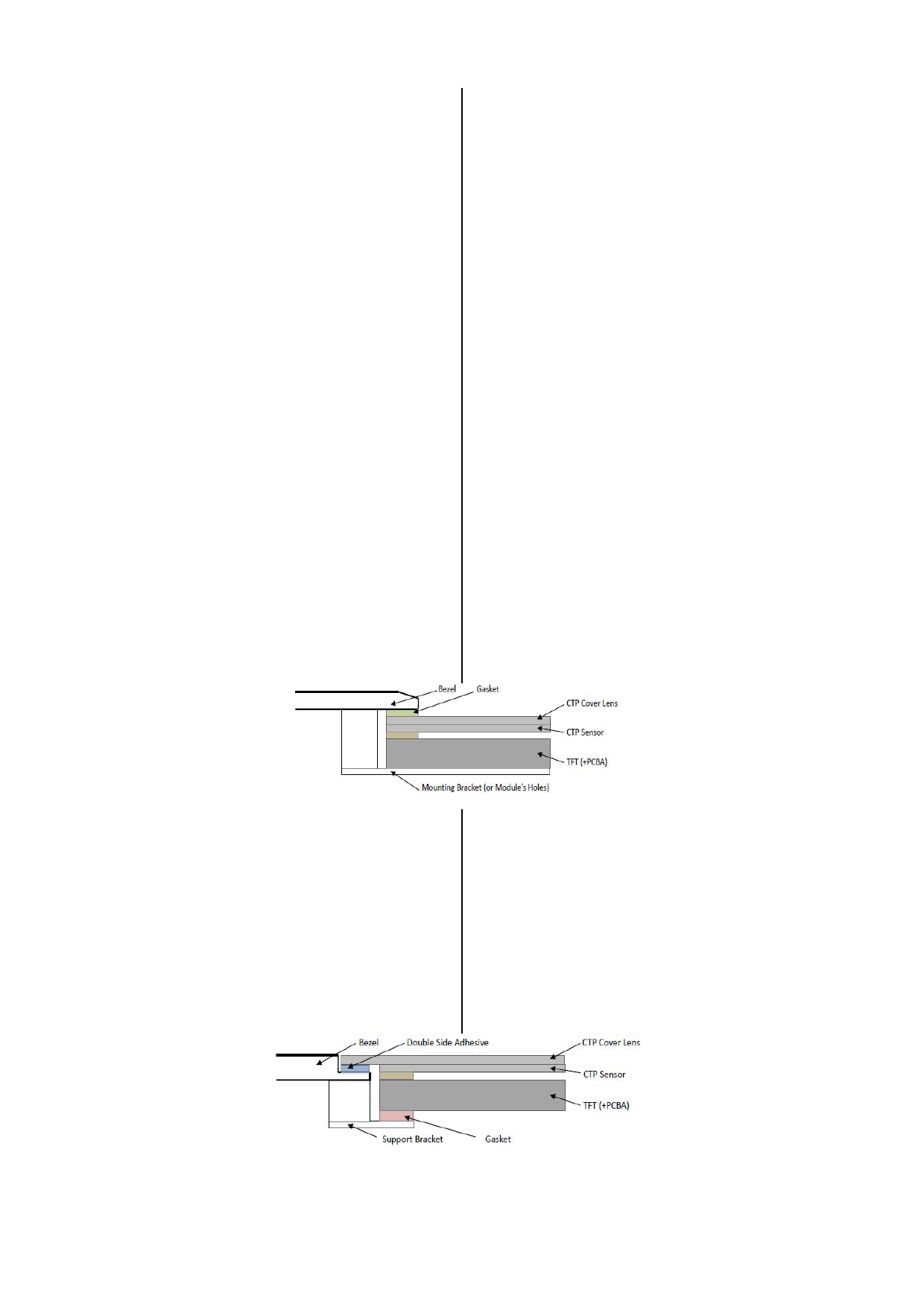
9.1 Bezel Mounting (Figure 1)
9.1 面框安装(附图 1 )
- The bezel window should be bigger than the CTP active area. It - 客户面框窗口应大于 CTP 动作区域,各边离动作区应
should be ≥ 0.5mm each side.
≥ 0.5mm 。
- Gasket should be installed between the bezel and the CTP surface. - 面框与 CTP 面板间应垫有胶垫,其最终间隙约为 0.5 ~
The final gap should be about 0.5~1.0mm.
1.0mm 。
- It is recommended to provide an additional support bracket for - 建议必要时在背面提供附加支架 ( 例如无安装结构的薄
backside support when necessary (e.g. slim type TFT module
型 TFT 模块 ) ,应仅利用适当支撑以保持模块位置。
without mounding structure). They should only provide appropriate
support and keep the module in place.
- The mounting structure should be strong enough to prevent - 安装结构应具有足够的强度,以防止外部不均匀力或
external uneven force or twist act onto the module.
扭曲力作用到模块上。
Figure 1
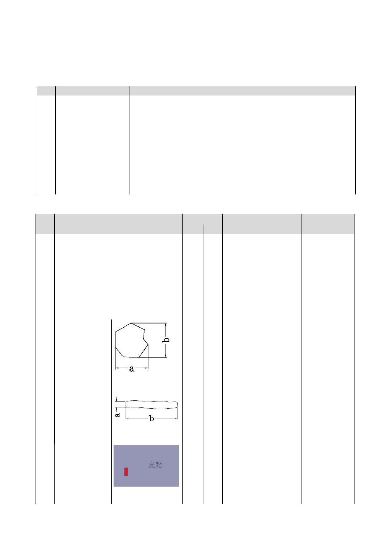
9.2 Surface Mounting (Figure 2)
9.2 嵌入安装(附图 2 )
- As the CTP assembling on the countersink area with double side - 客户面框应具有使用双面胶粘贴 CTP 的结构沉台面,
adhesive.The countersink area should be flat and clean to ensure
其粘贴面要求平整且洁净无污以保证粘贴牢靠。
the double side adhesive installation result.
- The Bezel is recommend to keep a gap ( ≥ 0.3mm each side) - 考虑到制作误差,建议面框与 CTP 盖板之间四周留有
around the cover lens for tolerance.
≥ 0.3mm 间隙。
- It is recommended to provide an additional support bracket with - 建议必要时在背面提供垫有胶垫附加支架 ( 例如无安装
gasket for backside support when necessary (e.g. TFT module
结构的 TFT 模块 ) ,应仅利用适当支撑以保持模块位
without mounding structure). They should only provide appropriate
置。
support and keep the module in place.
- The mounting structure should be strong enough to prevent - 安装结构应具有足够的强度,以防止外部不均匀力或
external uneven force or twist act onto the module
扭曲力作用到模块上。
Figure 2
URL: www.topwaydisplay.com
Document Name: LMT101DNLFWD-NND10-Manual-Rev0.1.doc
Page: 15 of 18
TOPWAY
LCD Module User Manual
LMT101DNLFWD-NND10
10.TFT QA Standard
10.1 INSPECTION CONDITION 检验条件
Unless otherwise stated , all the inspections are carryout under the following condition
除非有特别的规定,检验条件按以下执行。
No. Items 项目
Conditions 条件
1
Lighting
Illumination: Appearance 300-700Lux
照明
环境亮度在 300~700LUX
2
Inspection Distance
30-40cm form the test sample , within normal viewing angle
检验距离
眼睛距显示器表面 30~40cm
3
Temperature
Room Temperature (25 ºC), no condensation
环境温度
室温( 25 度 ±5% ),无凝水
4
Viewing Angle
U/D: 45º/45º, L/R: 45º/45º
视角
前后 45 度角范围内,左右 45 度角范围内
5
Inspection Time
15 seconds
检验时间
15 秒内
6
Defect Allowance
6 max
缺陷总数
允许 6 个
10.2 Display Pattern 显示缺陷
Type 类别
No. Items /Contents 检查项目
MA
MI Standard 标准
Judgment 判定
1
No Display
√
--
Not Allowed
无显示
不允许
2
Line defect
√
--
Not Allowed
缺少行或列
不允许
3
Display abnormally
√
--
Not Allowed
错误的显示
不允许
4
Function Defective
√
--
Not Allowed
缺少功能
不允许
5
Glass Crack
√
--
Not Allowed
玻璃破碎
不允许
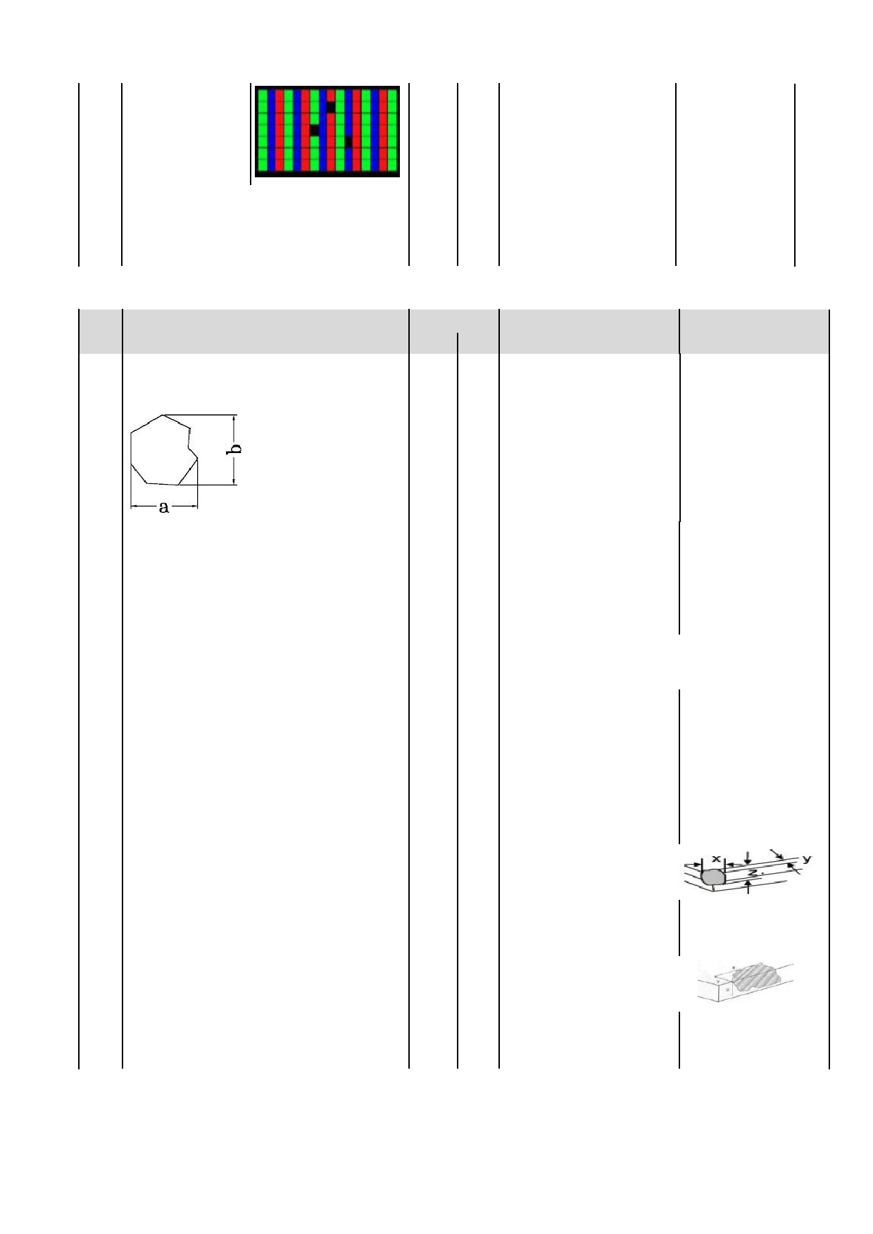
Spot Defect
√
(a+b)/2≤0.25
Allowed
6
Including ( Inside
允许
AA ) :
Black spot, White
0.25<(a+b)/2≤0.5
4 max.
spot , Foreign
允许 4 个
particle, Polarizer
(a+b)/2 > 0.5
Not Allowed
dirt, Cell particle
不允许
黑点 / 白点( AA
内)
7
Line Defect
√
a≤0.1
Allowed
Including ( Inside
允许
AA ) :
0.1<a≤0.2 and b≤5.0
4max.
Black line, White
允许 4 个
line,Scratch
线( AA 内)
a > 0.2 or b > 5.0
Not Allowed
不允许
9
Bright dot defect
√
Random
3 max.
允许 3 个
亮点
3 consecutive dots
Not Allowed
( 在全黑屏下多像
3 个或以上连续的点
不允许
素点)
URL: www.topwaydisplay.com
Document Name: LMT101DNLFWD-NND10-Manual-Rev0.1.doc
Page: 16 of 18
TOPWAY
LCD Module User Manual
LMT101DNLFWD-NND10
10
Dark dot defect
√
Random
5 max.
允许 5 个
暗点
3 consecutive dots
Not Allowed
(在全红或全绿或
3 个或以上连续的点
不允许
全蓝屏下缺像素
点)
13
Bright dot defect + Dark dot defect
√
--
5 max.
亮点 + 暗点
允许 5 个
15
PCBA defect
--
--
Refer to IPC-A-610
--
PCBA 缺陷
按照 IPC-A-610
10.3 Exterior 外观缺陷
Type 类别
No. Items /Contents 检查项目
MA
MI Standard 标准
Judgment 判定
1
Polarizer Dent/Bubble ( Inside AA ):
√
(a+b)/2≤0.3
Ignore
偏光片气泡
忽略
( AA 内)
0.3< (a+b)/2≤0.6
3 max.
允许 3 个
(a+b)/2 > 0.7
Not Allowed
不允许
2
FPC
√
Broken
Not Allowed
破损
不允许
√
naked wire 、 hole
Not Allowed
裸线、孔洞
不允许
3
Bezel scratches, pits,
√
Do not affect display, assembly, ignore.
bumps, Don't try dirt
不影响显示,组装则忽略
外框划痕、凹点、凸点、脏污
4
Protective film
√
Top injury 、 scratch 、 ignore
保护膜
Wear scar
忽略
Undamaged Polarizer ,
顶伤、擦伤、磨损
未损坏偏光片
dirt, particle
ignore
脏污
忽略
5
TP/Glass defect
√
1. Corner Fragment:
触摸屏、显示屏损伤
崩角
X≤2mm ; Y≤2mm ;
Ignore
Z≤T ( Glass
忽略
thickness )
2. Side Fragment:
崩边
X≤3.0mm ; Y ≤3.0mm ;
Ignore
Z≤T ( Glass
忽略
thickness )
URL: www.topwaydisplay.com
Document Name: LMT101DNLFWD-NND10-Manual-Rev0.1.doc
Page: 17 of 18

TOPWAY
LCD Module User Manual
LMT101DNLFWD-NND10
10.4 Quality Level and Sampling 抽样方法
Items 项目
Standard 标准
Sampling Standard 引用标准
MIL-STD-105E
Sampling Level 抽样等级
Ⅱ
AQL level 合格判定水平
MA: AQL=0.65
MI: AQL=1.0
Warranty
This product has been manufactured to our company’s specifications as a part for use in your company’s general
electronic products. It is guaranteed to perform according to delivery specifications. For any other use apart from general
electronic equipment, we cannot take responsibility if the product is used in medical devices, nuclear power control
equipment, aerospace equipment, fire and security systems, or any other applications in which there is a direct risk to
human life and where extremely high levels of reliability are required. If the product is to be used in any of the above
applications, we will need to enter into a separate product liability agreement.
- We cannot accept responsibility for any defect, which may arise form additional manufacturing of the product (including
disassembly and reassembly), after product delivery.
- We cannot accept responsibility for any defect, which may arise after the application of strong external force to the
product.
- We cannot accept responsibility for any defect, which may arise due to the application of static electricity after the
product has passed our company’s acceptance inspection procedures.
- When the product is in CCFL models, CCFL service life and brightness will vary according to the performance of the
inverter used, leaks, etc. We cannot accept responsibility for product performance, reliability, or defect, which may arise.
- We cannot accept responsibility for intellectual property of a third party, which may arise through the application of our
product to our assembly with exception to those issues relating directly to the structure or method of manufacturing of
our product.
URL: www.topwaydisplay.com
Document Name: LMT101DNLFWD-NND10-Manual-Rev0.1.doc
Page: 18 of 18