
LMT185EBKFDA
LCD Module User Manual
Prepared by:
Checked by:
Approved by:
Chenzhonghua
Date: 2024-03-16
Date:
Date:
Rev. Descriptions
Edit
Release Date
0.1
Preliminary
Chenzhonghua
2024-03-16
NURL: www.topwaydisplay.com
Document Name: LMT185EBKFDA-Manual-Rev0.1.doc
Page: 1 of 17

TOPWAY
LCD Module User Manual
LMT185EBKFDA
Table of Content
1. General Description........................................................................................................... 3
1.1 Introduction.............................................................................................................................................3
1.2 Features .............................................................................................................................................3
1.3 Application.............................................................................................................................................. 3
1.4 General Specification.............................................................................................................................4
2. Terminal Function.............................................................................................................. 5
2.1 Electrical Interface Connection..............................................................................................................5
2.2 LED Light Bar.........................................................................................................................................6
3. Absolute Maximum Ratings.............................................................................................. 6
3.1 Driving TFT LCD Panel..........................................................................................................................6
4. Electrical Characteristics.................................................................................................. 7
4.1 Electrical Specifications......................................................................................................................... 7
4.2 Backlight Unit......................................................................................................................................... 8
5. LVDS Interface....................................................................................................................9
6. Timing Chart..................................................................................................................... 10
6.1 AC Characteristics(LVDS)....................................................................................................................10
6.2 LVDS Rx Interface Timing Parameter..................................................................................................11
6.3 Sync Timing Waveforms...................................................................................................................... 12
6.4 Vertical Timing Waveforms.................................................................................................................. 12
6.5 Horizontal Timing Waveforms..............................................................................................................12
7. Input signals,Basic display colors &Grayscale of colors.............................................13
8. Power Sequence.............................................................................................................. 14
9. Optical Characteristics.................................................................................................... 14
9.1 Overview...............................................................................................................................................14
9.2 Optical Characteristics.........................................................................................................................15
10. Mechanical characteristics............................................................................................17
11. Warranty..........................................................................................................................17
NURL: www.topwaydisplay.com
Document Name: LMT185EBKFDA-Manual-Rev0.1.doc
Page: 2 of 17
TOPWAY
LCD Module User Manual
LMT185EBKFDA
1. General Description
1.1 Introduction
LMT185EBKFDA is a color active matrix TFT LCD module using amorphous silicon
TFT's (Thin Film Transistors) as an active switching devices. This module has a 18.5
inch diagonally measured active area with WXGA resolutions (1366 horizontal by 768
vertical
pixel array). Each pixel is divided into RED, GREEN, BLUE dots which are arranged
in vertical stripe and this module can display 16.7M colors. The TFT-LCD panel used
for this module is adapted for a low reflection and higher color type.
1.2 Features
LVDS Interface with 1 pixel / clock
High-speed response
Low power consumption
6-bit (Hi-FRC) color depth, display 16. 7M colors
Incorporated edge type back-light (One Light Bar)
High luminance and contrast ratio, low reflection and normal viewing angle
DE (Data Enable) only
RoHS
ES 6.0 compliant
Gamma correction
1.3 Application
Desktop Type of PC & Workstation Use
Slim-Size Display for Stand-alone Monitor
Display Terminals for Control System
Monitors for Process Controller
NURL: www.topwaydisplay.com
Document Name: LMT185EBKFDA-Manual-Rev0.1.doc
Page: 3 of 17

TOPWAY
LCD Module User Manual
LMT185EBKFDA
1.4 General Specification
Parameter
Specification
Unit
Remarks
Active area
409.8(H) × 230.4(V)
mm
Number of pixels
1366(H) × 768(V)
pixels
Pixel pitch
0.1(H) ×0.3(V)
mm
Pixel arrangement
RGB Vertical stripe
Display colors
16.7M
colors
Display mode
Normally Black
Dimensional outline
430.4(H) ×254.6(V) ×10.9(D) typ.
mm
Detail refer to drawing
Weight
1300(typ.)
g
Bezel width (L/R/U/D) 8.5/8.5/10.3/10.3
mm
Surface Treatment
Haze 25%, 3H
Back-light
rightedge side, 1-LED Light bar
NURL: www.topwaydisplay.com
Document Name: LMT185EBKFDA-Manual-Rev0.1.doc
Page: 4 of 17

TOPWAY
LCD Module User Manual
LMT185EBKFDA
2. Terminal Function
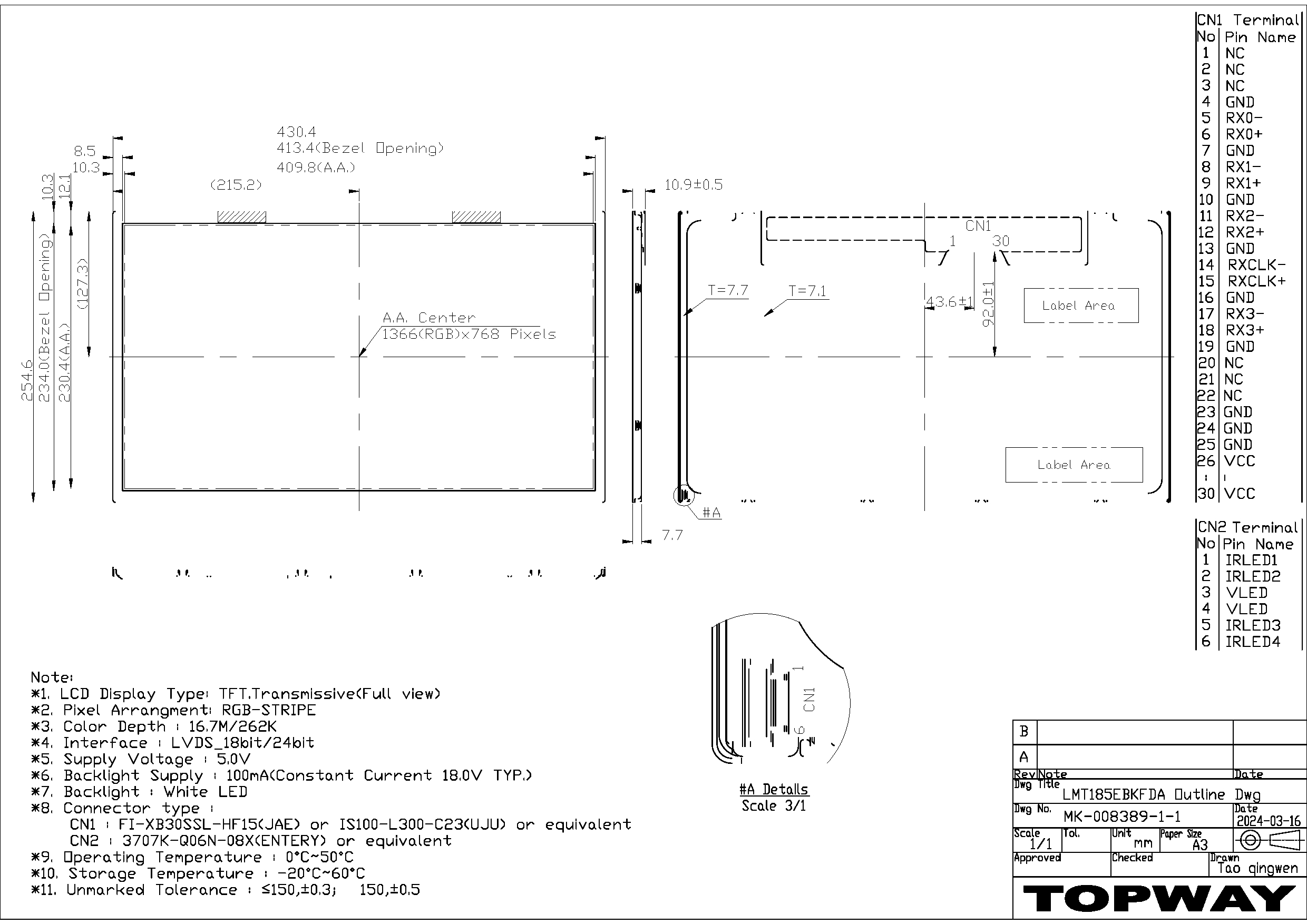
2.1 Electrical Interface Connection
CN1
Module Side Connector : UJU IS100-30O-C23 or Equivalent
User Side Connector : JAE FI-X30H or Equivalent
Pin No
Symbol
Function
Remark
1
NC
No connection
2
NC
No connection
3
NC
No connection
4
GND
GND Ground
5
RX0-
Negative LVDS differential data input. Channel 0
6
RX0+
Positive LVDS differential data input. Channel 0
7
GND
Ground
Optical: Bist function
8
RX1-
Negative LVDS differential data input. Channel 1
9
RX1+
Positive LVDS differential data input. Channel 1
10
GND
Ground
11
RX2-
Negative LVDS differential data input. Channel 2
12
RX2+
Positive LVDS differential data input. Channel 2
13
GND
Ground
14
RXCLK-
Negative LVDS differential clock input.
15
RXCLK+
Positive LVDS differential clock input.
16
GND
Ground
17
RX3-
Negative LVDS differential data input. Channel 3
18
RX3+
Positive LVDS differential data input. Channel 3
19
GND
Ground
20
NC
Not connection, this pin should be open.
21
NC
Not connection, this pin should be open.
22
NC
Not connection, this pin should be open.
23
GND
Ground
24
GND
Ground
25
GND
Ground
26
VCC
5V Power supply
27
VCC
28
VCC
29
VCC
30
VCC
NURL: www.topwaydisplay.com
Document Name: LMT185EBKFDA-Manual-Rev0.1.doc
Page: 5 of 17

TOPWAY
LCD Module User Manual
LMT185EBKFDA
2.2 LED Light Bar
-LED connector : 3708K-Q06N-00R manufactured by Entry
Pin No
Symbol
Description
1
IRLED1
LED current sense for string1
2
IRLED2
LED current sense for string2
3
VLED
LED power supply
4
VLED
LED power supply
5
IRLED3
LED current sense for string3
6
IRLED4
LED current sense for string4
3. Absolute Maximum Ratings
3.1 Driving TFT LCD Panel
Symbol
Min.
Max.
Unit
Remarks
Parameter
Power Supply Voltage
V DD
-0.3
5.5
V
Ta = 25 ℃
Logic Supply Voltage
V IN
VSS-0.3
V DD +0.3
V
LED Channel Current
I BL
-
85
mA
Operating Temperature
T OP
0
+50
℃
1)
Storage Temperature
T ST
-20
+60
℃
1)
Note : 1) Temperature and relative humidity range are shown in the figure below.
Wet bulb temperature should be 39 OC max. and no condensation of water.
NURL: www.topwaydisplay.com
Document Name: LMT185EBKFDA-Manual-Rev0.1.doc
Page: 6 of 17

TOPWAY
LCD Module User Manual
LMT185EBKFDA
4. Electrical Characteristics
4.1 Electrical Specifications
[Ta =25± 2 ℃ ]
Parameter
Min.
Typ.
Max.
Unit
Remarks
Power Supply Voltage
V DD
4.5
5.0
5.5
V
Note1
Power Supply Current
I DD
-
500
720
mA
In-Rush Current
I RUSH
-
2
3
A
Note 2
Permissible Input Ripple
V RF
-
-
300
mV
Note1,3
Voltage
High Level Differential Input
V IH
-
-
+100
mV
Threshold Voltage
Low Level Differential Input
V IL
-100
-
-
mV
Threshold Voltage
Differential input voltage
|V ID |
200
-
600
mV
Differential input common mode Vcm
1.0
1.2
1.5
V IH =100mV,
voltage
V IL =-100mV
LED ChannelVoltage
V L
17.4
18
19.8
V
LED Channel Current
I L
-
100
-
mA
LED Lifetime
30,000
-
-
Hrs
Power Consumption
P D
-
2.5
3.6
W
@60Hz
P BL
-
7.2
7.92
W I L =100mA, Note 4
P total
-
8.62
10.33
W
Notes : 1. The supply voltage is measured and specified at the interface connector of LCM.
The current draw and power consumption specified is for VDD=5.0V, Frame rate=60Hz and
Clock frequency = 75.4MHz. Test Pattern of power supply current
a) Typ : Color Bar pattern
b) Max: Gray Level 255
2.Duration of rush current is about 2 ms and rising time of VDD is 520 μs ± 20 %
3.Ripple Voltage should be covered by Input voltage Spec.
4.Calculated value for reference (VL × IL ) × 4(channel) excluding driver loss. (LED Light bar: 6S4P)
NURL: www.topwaydisplay.com
Document Name: LMT185EBKFDA-Manual-Rev0.1.doc
Page: 7 of 17

TOPWAY
LCD Module User Manual
LMT185EBKFDA
4.2 Backlight Unit
Parameter
Min.
Typ.
Max.
Unit
Remarks
LED Light Bar Input Voltage
Per Input Pin
VPIN
17.4
18
19.8
V
Duty 100%
LED Light Bar Input Cuttent
Per Input pin
IPIN
-
100
-
mA
LED Power Consumption
P BL
-
7.2
7.92
W
Note 3
LED Life-Time
-
30,000
-
Hrs
Note 4
LED bar consists of 24LED packages,4 strings(parallel)*6packages(serial)
Note1: There are one light bar ,and the specified current is input LED chip 100% duty current
Note2: The sense current of each input pin is 100mA
Note3: PBL=4 Input pins*VPIN × IPIN
Note4: The lifetime is determined as the time at which luminance of LED become 50% of the initial
brightness or not normal lighting at IPIN=85mA on condition of continuous operating at
25 ± 2 ℃
NURL: www.topwaydisplay.com
Document Name: LMT185EBKFDA-Manual-Rev0.1.doc
Page: 8 of 17

TOPWAY
LCD Module User Manual
LMT185EBKFDA
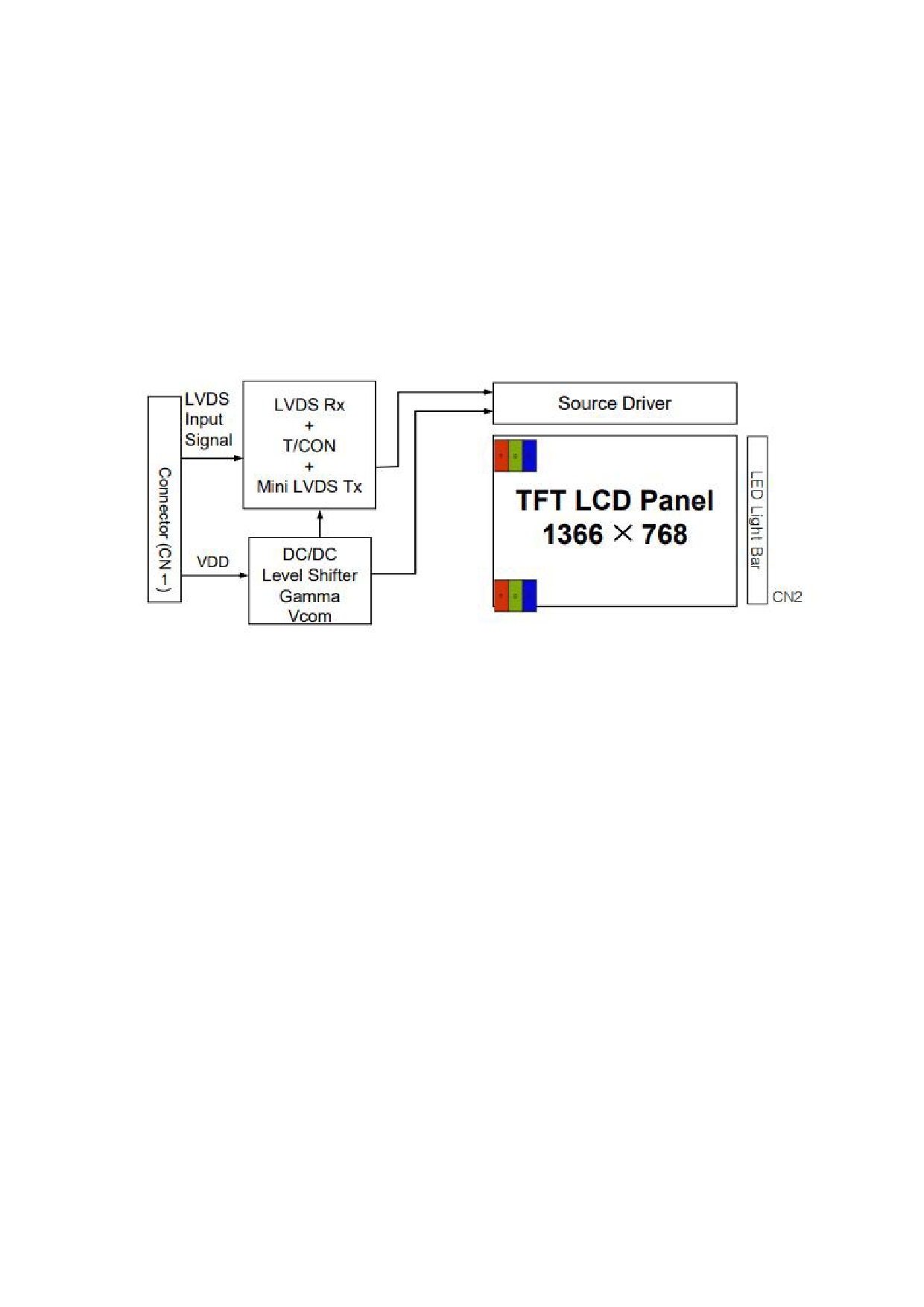
5. LVDS Interface
LMT185EBKFDA
Transmitter
Interface
Remark
(CN11)
Input Signal
Pin No.
Pin No. System (Tx)
TFT-LCD
(Rx)
Pin No.
OR0
51
OR1
52
OR2
54
OR3
55
48
RXO0-
5
47
OUT0- OUT0+
RXO0+
6
OR4
56
OR5
3
OG0
4
OG1
6
OG2
7
OG3
11
OG4
12
46
OUT1-
RXO1-
8
45
OUT1+
RXO1+
9
OG5
14
OB0
15
L
OB1
19
V
OB2
20
D
S
OB3
22
OB4
23
OB5
24
42
OUT2-
RXO2-
11
41
OUT2+
RXO2+
12
Hsync
27
Vsync
28
DE
30
MCLK
31
40
CLK OUT-
RXO CLK-
14
39
CLK OUT+
RXO CLK+
15
OR6
50
OR7
2
OG6
8
OG7
10
38
OUT3-
RXO3-
17
37
OUT3+
RXO3+
18
OB6
16
OB7
18
RSVD
25
NURL: www.topwaydisplay.com
Document Name: LMT185EBKFDA-Manual-Rev0.1.doc
Page: 9 of 17

TOPWAY
LCD Module User Manual
LMT185EBKFDA
6. Timing Chart
6.1 AC Characteristics(LVDS)
Item
Symbols
Min
Typ
Max
Unit
DCLK
Period
tCLK
10.6
13.26
15.91
ns
Frequency
-
62.9
75.4
94.3
MHz
Horizontal
Period
tHP
1446
1560
1936
tCLK
Display
Term
Horizontal Valid
tHV
1366
1366
1366
tCLK
Horizontal Blank
tHB
80
194
570
tCLK
Frequency
fH
40.3
48.36
60.45
KHz
Vertical
Period
tVP
778
806
888
tHP
Display
Term
Vertical Valid
tVV
768
768
768
tHP
Vertical Blank
tVB
10
38
120
tHP
Frequency
fV
50
60
75
Hz
LVDS
Input spread
SSr
-3
-
+3
%
Receiver
clock
spectrum ratio
Note: The DCLK range at last line of V-blanking should be set in 0~987
NURL: www.topwaydisplay.com
Document Name: LMT185EBKFDA-Manual-Rev0.1.doc
Page: 10 of 17
TOPWAY
LCD Module User Manual
LMT185EBKFDA
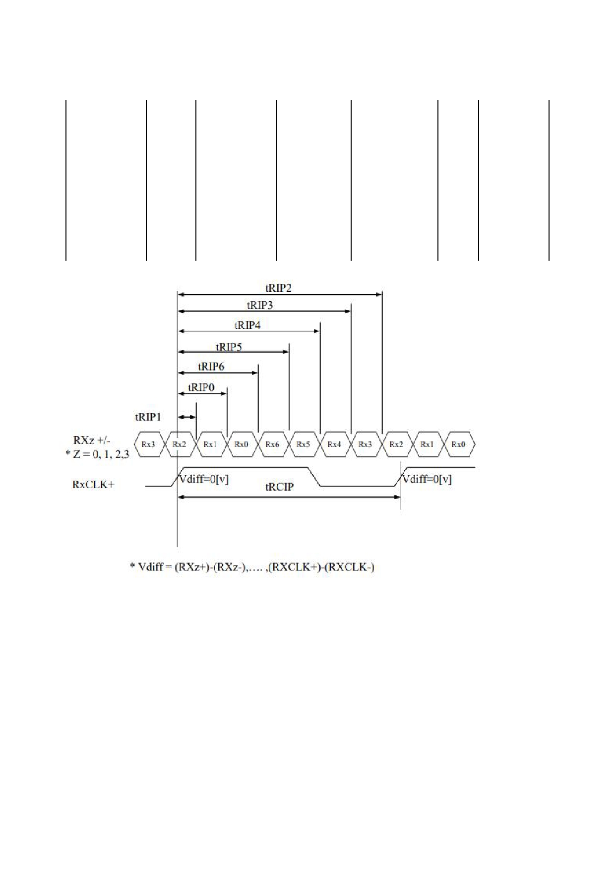
6.2 LVDS Rx Interface Timing Parameter
The specification of the LVDS Rx interface timing parameter is shown.
Item
Symbol
Min
Typ
Max
Unit
Remark
CLKIN Period
tRCIP
10.60
13.26
15.91
nsec
Input Data 0
tRIP1
-0.4
0.0
+0.4
nsec
Input Data 1
tRIP0
tRCIP/7-0.4
tRCIP/7
tRCIP/7+0.4
nsec
Input Data 2
tRIP6
2 ×tRCIP/7-0.4
2 ×tRCIP/7
2 ×tRCIP/7+0.4
nsec
Input Data 3
tRIP5
3 ×tRCIP/7-0.4
3 ×tRCIP/7
3 ×tRCIP/7+0.4
nsec
Input Data 4
tRIP4
4 ×tRCIP/7-0.4
4 ×tRCIP/7
4 ×tRCIP/7+0.4
nsec
Input Data 5
tRIP3
5 ×tRCIP/7-0.4
5 ×tRCIP/7
5 ×tRCIP/7+0.4
nsec
Input Data 6
tRIP2
6 ×tRCIP/7-0.4
6 ×tRCIP/7
6 ×tRCIP/7+0.4
nsec
NURL: www.topwaydisplay.com
Document Name: LMT185EBKFDA-Manual-Rev0.1.doc
Page: 11 of 17

TOPWAY
LCD Module User Manual
LMT185EBKFDA
6.3 Sync Timing Waveforms
1) Need over 3 H-sync during V-Sync Low
2) Fix H-Sync width from V-Sync falling edge to first rising edge
6.4 Vertical Timing Waveforms
6.5 Horizontal Timing Waveforms
NURL: www.topwaydisplay.com
Document Name: LMT185EBKFDA-Manual-Rev0.1.doc
Page: 12 of 17
TOPWAY
LCD Module User Manual
LMT185EBKFDA
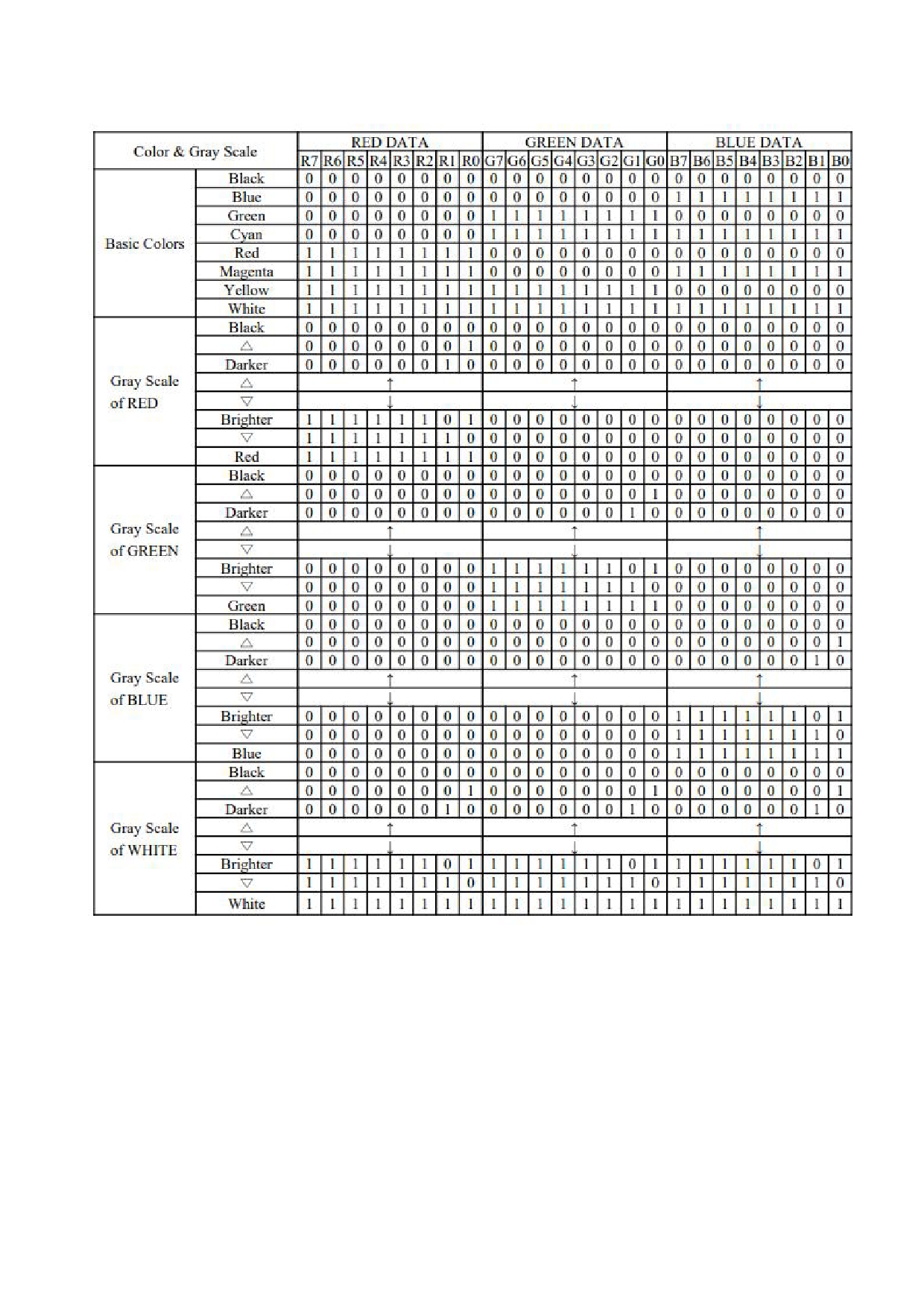
7. Input signals,Basic display colors &Grayscale of colors
NURL: www.topwaydisplay.com
Document Name: LMT185EBKFDA-Manual-Rev0.1.doc
Page: 13 of 17
TOPWAY
LCD Module User Manual
LMT185EBKFDA
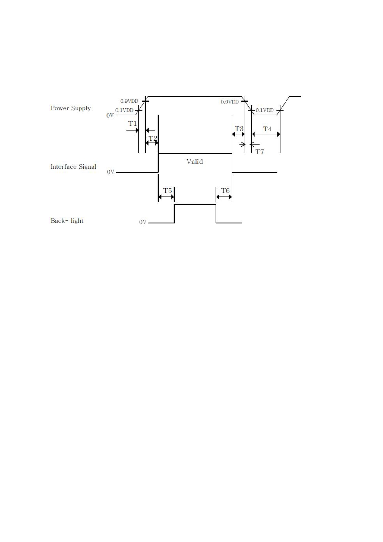
8. Power Sequence
To prevent a latch-up or DC operation of the LCD module, the power on/off sequence s
hall be as shown in below
0.5 ms ≤ T1≤10ms
0 ≤T2 ≤50 ms
0 ≤ T3 ≤50 ms
1sec ≤ T4
200 ms ≤T5
200 ms ≤T6
Notes:
1. When the power supply VDD is 0V, keep the level of input signals on
the low or keep high impedance.
2. Do not keep the interface signal high impedance when power is on.
3. Back Light must be turn on after power for logic and interface signal are valid.
4. T7 decreases smoothly, there is none re-bouncing voltage.
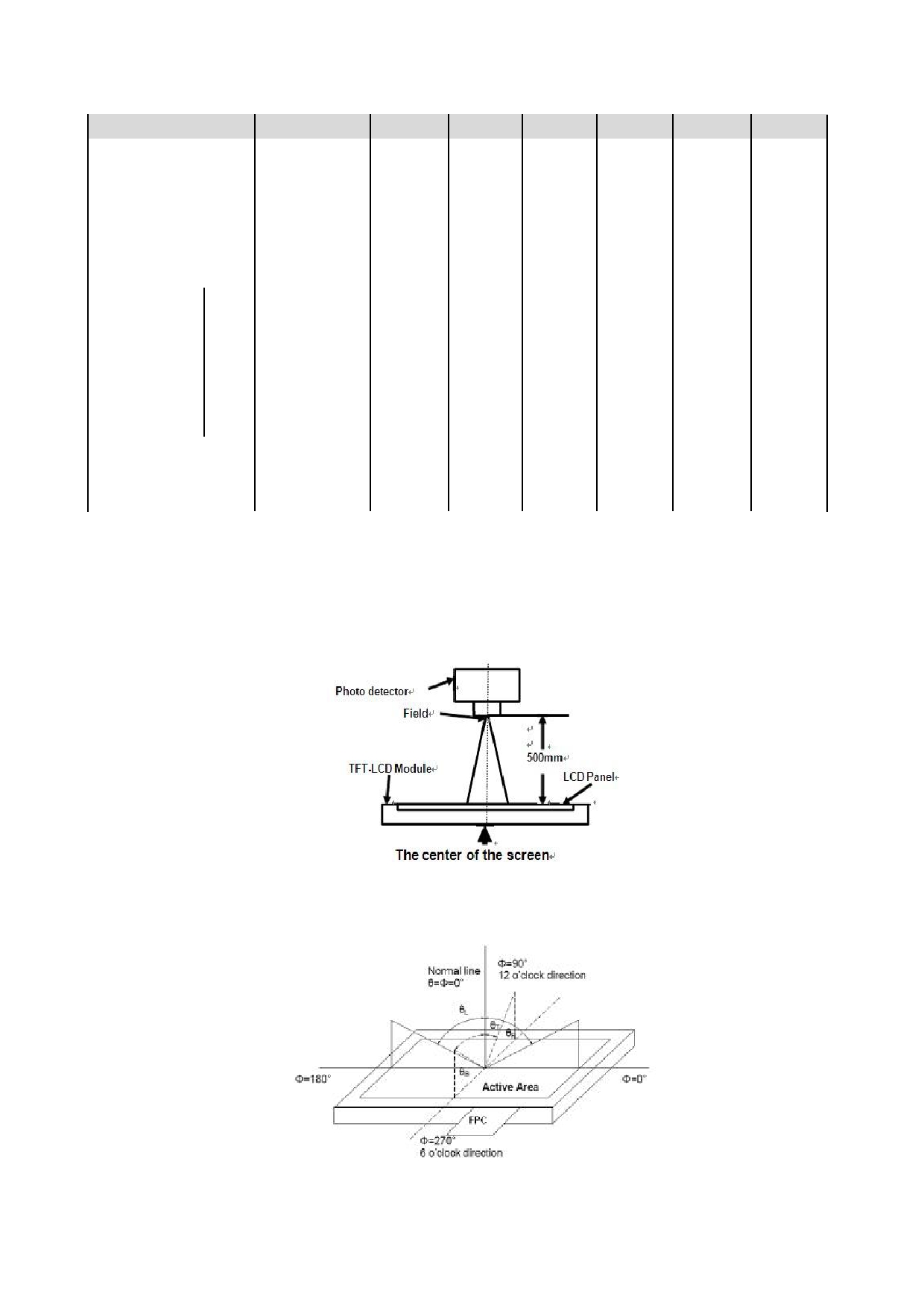
9. Optical Characteristics
9.1 Overview
The test of Optical specifications shall be measured in a dark room (ambient luminance ≤1
lux and temperature = 25 ± 2 ℃ ) with the equipment of Luminance meter system (Goniometer system and
TOPCONE PR730) and test unit shall be located at an approximate distance 50cm from the LCD surface at a
viewing angle of θ and Φ equal to 0. We refer to θ Ø=0 (=θ 3 ) as the 3 o’clock direction (the “right”), θ Ø=90 (= θ 12 ) as
the 12 o’clock direction (“upward”), θ Ø=180 (= θ 9 ) as the 9 o’clock direction (“left”) and θ Ø=270 (= θ 6 ) as the 6
o’clock direction (“bottom”). While scanning θ and/or Ø, the center of the measuring spot on the Display
surface shall stay fixed. The measurement shall be executed after 30 minutes warm-up period. VDD shall be
5.0V +/-10% at 25 ℃ . Optimum viewing angle direction is 6 ’clock
NURL: www.topwaydisplay.com
Document Name: LMT185EBKFDA-Manual-Rev0.1.doc
Page: 14 of 17
TOPWAY
LCD Module User Manual
LMT185EBKFDA
9.2 Optical Characteristics
Item
Symbol
Conditi
Min
Typ
Max
Unit Remark
θT
on
85
89
-
View Angles
θB
CR ≧ 10
85
89
-
Degree
Note 2
θL
85
89
-
θR
85
89
-
Contrast Ratio
CR
θ=0°
700
1000
-
-
Note1
Note3
Response Time
TON+TOFF
25 ℃
-
15
25
ms
Note1
Note4
White
x
0.283
0.313
0.343
y
0.299
0.329
0.359
Red
x
0.638
0.658
0.688
y
Backlight
0.308
0.338
0.368
Chromaticity
Note5
x
is
0.267
0.297
0.327
-
Green
Note1
y
on
0.627
0.657
0.687
Blue
x
0.122
0.152
0.182
y
0.040
0.070
0.100
Uniformity
U
-
75
80
-
%
Note1
Note6
Luminance
L
-
200
250
-
cd/m 2
Note1
Note7
Test Conditions:
1. The ambient temperature is 25±2 ℃ .humidity is 65±7%
2. The test systems refer to Note 1 and Note 2.
Note 1: Definition of optical measurement system.
The optical characteristics should be measured in dark room. After 5 Minutes operation, the optical
properties are measured at the center point of the LCD screen. All input terminals LCD panel must
be ground when measuring the center area of the panel.
Note 2: Definition of viewing angle range and measurement system.
viewing angle is measured at the center point of the LCD.
Note 3:Definition of contrast ratio
NURL: www.topwaydisplay.com
Document Name: LMT185EBKFDA-Manual-Rev0.1.doc
Page: 15 of 17
TOPWAY
LCD Module User Manual
LMT185EBKFDA
“White state”: The state is that the LCD should driven by Vwhite.
“Black state”: The state is that the LCD should driven by Vblack.
Vwhite: To be determined
Vblack: To be determined.
Note 4:Definition of Response time
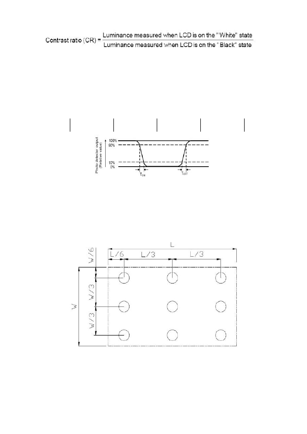
The response time is defined as the LCD optical switching time interval between “White” state and “Black” state.
Rise time (TON) is the time between photo detector output intensity changed from 90% to 10%. And fall time
(TOFF) is the time between photo detector output intensity changed from 10% to 90%.
White (TFT
Black (TFT
White (TFT
off)
on)
off)
Note 5: Definition of color chromaticity (CIE1931)
Color coordinates measured at center point of LCD.
Note 6: Definition of Luminance Uniformity
Active area is divided into 9 measuring areas (Refer Fig. 2). Every measuring point is placed at the
center of each measuring area.
L-------Active area length
W----- Active area width
Luminance Uniformity (U) = Lmin/ Lmax
Lmax: The measured Maximum luminance of all measurement position.
Lmin: The measured Minimum luminance of all measurement position.
Note 7: Definition of Luminance:
Measure the luminance of white state at center point.
NURL: www.topwaydisplay.com
Document Name: LMT185EBKFDA-Manual-Rev0.1.doc
Page: 16 of 17

TOPWAY
LCD Module User Manual
LMT185EBKFDA
10. Mechanical characteristics
Parameter
Specification
Unit
Dimensional outline
430.4 × 254.6× 10.9
mm
Weight
1300(typ.)
gram
Active area
409.8(H) × 230.4(V)
mm
Pixel pitch
0.1(H) × 0.3(V)
mm
Number of pixels
1366(H)× 768(V) (1 pixel = R + G + B dots)
pixels
Back-light
Right edge side 1-LED Light bar Type
11. Warranty
This product has been manufactured to our company’s specifications as a part for use in your company’s general electronic
products. It is guaranteed to perform according to delivery specifications. For any other use apart from general electronic
equipment, we cannot take responsibility if the product is used in medical devices, nuclear power control equipment,
aerospace equipment, fire and security systems, or any other applications in which there is a direct risk to human life and
where extremely high levels of reliability are required. If the product is to be used in any of the above applications, we will
need to enter into a separate product liability agreement.
- We cannot accept responsibility for any defect, which may arise form additional manufacturing of the product (including
disassembly and reassembly), after product delivery.
- We cannot accept responsibility for any defect, which may arise after the application of strong external force to the
product.
- We cannot accept responsibility for any defect, which may arise due to the application of static electricity after the
product has passed our company’s acceptance inspection procedures.
- When the product is in CCFL models, CCFL service life and brightness will vary according to the performance of the
inverter used, leaks, etc. We cannot accept responsibility for product performance, reliability, or defect, which may arise.
-
We cannot accept responsibility for intellectual property of a third part, which may arise through the application of
our product to our assembly with exception to those issues relating directly to the structure or method of manufacturing
of our product.
NURL: www.topwaydisplay.com
Document Name: LMT185EBKFDA-Manual-Rev0.1.doc
Page: 17 of 17
>