
+86(755)3699-5528
Shenzhen TOPWAY Technology Co., Ltd.
+86(755)8179-5700
Model No.TM101DDHG04
MODEL NO. :
TM101DDHG04
ISSUED DATE:
2017-03-31
VERSION
:
Ver 2.0
□ Preliminary Specification
■ Final Product Specification
Customer :
Approved by
Notes
TIANMA Confirmed :
Prepared by
Checked by
Approved by
Haiping_luo
Guangkun_an
This technical specification is subjected to change without notice
The information contained herein is the exclusive property of TIANMA MICRO-ELECTRONICS Corporation
and shall not be distributed, reproduced, or disclosed in whole or in part without prior written permission of
TIANMA MICRO-ELECTRONICS Corporation.
Page 1 of 42
www.topwaydisplay.com
sales@topwaydisplay.com

+86(755)3699-5528
Shenzhen TOPWAY Technology Co., Ltd.
+86(755)8179-5700
Model No.TM101DDHG04
Table of Contents
Record of Revision............................................................................................................................ 3
1 General Specifications ............................................................................................................... 4
2 Input/Output Terminals............................................................................................................... 5
3 Absolute Maximum Ratings ....................................................................................................... 6
4 Electrical Characteristics............................................................................................................ 7
5 Timing Chart............................................................................................................................. 10
6 Optical Characteristics ............................................................................................................. 16
7 Environmental / Reliability Test ................................................................................................ 19
8 Mechanical Drawing................................................................................................................. 19
9 Packing Drawing ...................................................................................................................... 26
10 Precautions for Use of LCD Modules ....................................................................................... 29
11 Outgoing Inspection Report ……………………………………………………………………….....30
12 QC flow chart ………………………………………………………………………...........................31
13 Incoming Inspection Standard ..................................................................................................36
The information contained herein is the exclusive property of TIANMA MICRO-ELECTRONICS Corporation
and shall not be distributed, reproduced, or disclosed in whole or in part without prior written permission of
TIANMA MICRO-ELECTRONICS Corporation.
Page 2 of 42
www.topwaydisplay.com
sales@topwaydisplay.com
+86(755)3699-5528
Shenzhen TOPWAY Technology Co., Ltd.
+86(755)8179-5700
Model No.TM101DDHG04
Record of Revision
Rev
Issued Date
Description
Editor
1.0
2016-12-13
Fin Specification Release
Jinzhao Xian
1.1
2016-01-13
Add rework QC flow chart in page 35
Jinzhao Xian
1.2
2016-01-18
Add Incoming Inspection Standard in page 36
Add Customer G-code in page 27
Jinzhao Xian
2.0
2017-03-31
Update pin defination
Haiping_luo
The information contained herein is the exclusive property of TIANMA MICRO-ELECTRONICS Corporation
and shall not be distributed, reproduced, or disclosed in whole or in part without prior written permission of
TIANMA MICRO-ELECTRONICS Corporation.
Page 3 of 42
www.topwaydisplay.com
sales@topwaydisplay.com
+86(755)3699-5528
Shenzhen TOPWAY Technology Co., Ltd.
+86(755)8179-5700
Model No.TM101DDHG04
1
General Specifications
1.1 Display Spec & Electrical Characteristics
Feature
Spec
Size
10.1 inch
Resolution
1024(RGB )× 600
Technology Type
a-si TFT
Pixel Configuration
R.G.B. Vertical Stripe
Pixel pitch(mm)
0.2175x0.2088
Display Spec.
Display Mode
TM, Normally White
Surface Treatment
AG,HC(3H)
Viewing Direction
12 o’clock
Gray Scale Inversion Direction
6 o’clock
With /Without TSP
Without TSP
LED Numbers
30 LED (JuFei)
Weight (g)
210(typ), 220 (max)
Interface
6/8 bit LVDS
Electrical
Characteristics
Color Depth
16.7M
Driver IC
HX8282*1+HX8677*2
Module Power Consumption(W)
2.43(max)
Note 1: Requirements on Environmental Protection: Q/S0002
Note 2: LCM weight tolerance: ± 5%
Note 3: Power Consumption measure at Black image
1.2 Mechanical Characteristics
Item
Min
Typ
Max
LCM (W x H x D) (mm) With Tape
232.85x136.85x2.8
233.1x137.1x3.05
233.35x137.35x3.3
Without Tape
232.8x136.8x2.8
233.0x137.0x3.0
233.2x137.2x3.2
Bezel Opening Area ( mm )
225.52x128.08
225.72x128.28
225.92x128.48
Active Area(mm)
222.52x125.08
222.72x125.28
222.92x125.48
The information contained herein is the exclusive property of TIANMA MICRO-ELECTRONICS Corporation
and shall not be distributed, reproduced, or disclosed in whole or in part without prior written permission of
TIANMA MICRO-ELECTRONICS Corporation.
Page 4 of 42
www.topwaydisplay.com
sales@topwaydisplay.com
+86(755)3699-5528
Shenzhen TOPWAY Technology Co., Ltd.
+86(755)8179-5700
Model No.TM101DDHG04
2
Input/Output Terminals
Recommended connector: IMSA-9637S-40Y801
Pin
Symbol
I/O
Description
Remark
1
VCOM
P
VCOM Power supply
2
VDD
P
Power supply(3.3V typ)
3
VDD
P
Power supply(3.3V typ)
4
NC
P
No connection(Reserved for TM test)
.
5
RESET ( GRB )
I
Global Reset.Normally pull high.
6
STBYB
I
Standby mode control.Normally pull high.
7
GND
P
Ground
8
Rxin0-
I
LVDS differential data input
9
Rxin0+
I
10
GND
P
Ground
11
Rxin1-
I
LVDS differential data input
12
Rxin1+
I
13
GND
P
Ground
14
Rxin2-
I
LVDS differential data input
15
Rxin2+
I
16
GND
P
Ground
17
RxCLK-
I
LVDS differential clock input
18
RxCLK+
I
19
GND
P
Ground
20
Rxin3-
I
LVDS differential data input
21
Rxin3+
I
22
GND
P
Ground
23
NC
No connection
24
NC
No connection
25
GND
P
Ground
26
NC
No connection
27
NC
No connection
The information contained herein is the exclusive property of TIANMA MICRO-ELECTRONICS Corporation
and shall not be distributed, reproduced, or disclosed in whole or in part without prior written permission of
TIANMA MICRO-ELECTRONICS Corporation.
Page 5 of 42
www.topwaydisplay.com
sales@topwaydisplay.com
+86(755)3699-5528
Shenzhen TOPWAY Technology Co., Ltd.
+86(755)8179-5700
Model No.TM101DDHG04
LVDS 6/8 bit selection control
28
SELB(HSD)
I
SEL=”L”:8bit Use only 8 bit
SEL=”h”:6bit Use only 6 bit
29
AVDD
P
Analog power
30
GND
P
Ground
31
LED-
P
Back light cathode
32
LED-
P
Source Driver internal shift register is
33
L/R
P
controlled by this pin as shown below:
Normally pull high.
34
U/D
I
Gate Driver Up/down Scan setting.Normally
pull low.
35
VGL
I
Negative power of TFT
36
NC
No connection
37
NC
No connection
38
VGH
P
Positive power of TFT
39
LED+
P
Back light anode
40
LED+
P
3
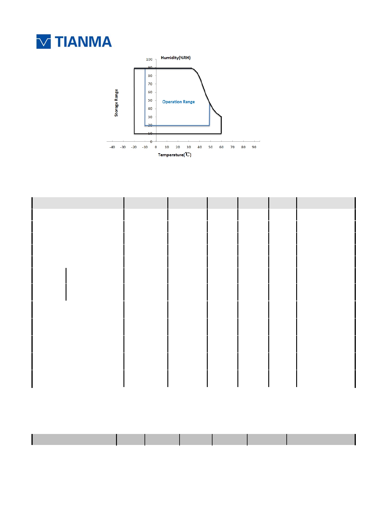
Absolute Maximum Ratings
GND=0V, Ta =25 ℃
Item
Symbol
Min
Max
Unit
Remark
Power Voltage
VDD
2.8
3.6
V
Operating Ambient Temperature
TOPR
-10
50
℃
Storage Ambient Temperature
TSTG
-20
60
℃
Operating and Storage Humidity
HSTG
10%
90%
% ( RH )
Note: LCM surface Temperature reach 60 ℃ is ok, When Operating condition.
The information contained herein is the exclusive property of TIANMA MICRO-ELECTRONICS Corporation
and shall not be distributed, reproduced, or disclosed in whole or in part without prior written permission of
TIANMA MICRO-ELECTRONICS Corporation.
Page 6 of 42
www.topwaydisplay.com
sales@topwaydisplay.com
+86(755)3699-5528
Shenzhen TOPWAY Technology Co., Ltd.
+86(755)8179-5700
Model No.TM101DDHG04
4
Electrical Characteristics
4.1 Driving TFT LCD Panel
VDD=3.3V, GND=0V, Ta=25 ℃
Item
Symbol
Min
Typ
Max
Unit
Remark
Power Supply Voltage
VDD
2.80
3.30
3.60
V
Power For Analog Circuit
AVDD
10.72
11.02
11.34
V
Gate On Voltage
VGH
20.46
21.14
23.54
V
Gate Off Voltage
VGL
-7.35
-7
-6.65
V
Common Voltage
Vcom
--
4.33
--
V
Input
Low Level
V IL
GND
--
0.2xVDD
V
Signal
Voltage
High Level
V IH
0.8xVDD
--
VDD
V
Current of digital supply
voltage
I VDD
--
--
22
mA
VDD=3.3V
Current of analog supply
voltage
I AVDD
--
--
40
mA
AVDD=11.02V
Current of Gate on voltage
I VGH
--
--
0.8
mA
VGH=21.14V
Current of Gate off voltage
I VGL
--
--
0.8
mA
VGL=-7.0V
Current of Vcom
Ivcom
--
--
0.01
mA
Note: The current of supply voltage measure at black image.
4.2 Driving Backlight
Ta=25 ℃
Item
Symbol
Min
Typ
Max
Unit
Remark
The information contained herein is the exclusive property of TIANMA MICRO-ELECTRONICS Corporation
and shall not be distributed, reproduced, or disclosed in whole or in part without prior written permission of
TIANMA MICRO-ELECTRONICS Corporation.
Page 7 of 42
www.topwaydisplay.com
sales@topwaydisplay.com
+86(755)3699-5528
Shenzhen TOPWAY Technology Co., Ltd.
+86(755)8179-5700
Model No.TM101DDHG04
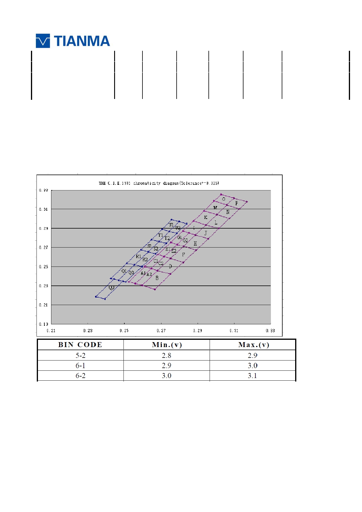
Forward Current
I F
--
200
--
mA
Forward Current Voltage
V F
8.4
9.0
9.45
V
30 LEDs(3 LED
Backlight Power
Serial,10 LED
Consumption
W BL
--
1800
--
mW
Parallel)
LED lifetime
--
15000
--
--
hrs
Note1: The LED driving condition is defined for each LED module (3 LED Serial,10 LED Parallel).
Note2: Under LCM operating, the stable forward current should be input. And forward voltage is
for reference only.
Note3: Optical performance should be evaluated at only Ta=25 ℃ ,If LED is driven by high current,
high ambient temperature & humidity condition, the life time of LED will be reduced.
Operating life means brightness goes down to 50% initial brightness. Typical operating life
time is estimated data.
Note4: LED C(C1+C2) chromaticity and BIN code 5-2~6-2.
The information contained herein is the exclusive property of TIANMA MICRO-ELECTRONICS Corporation
and shall not be distributed, reproduced, or disclosed in whole or in part without prior written permission of
TIANMA MICRO-ELECTRONICS Corporation.
Page 8 of 42
www.topwaydisplay.com
sales@topwaydisplay.com
+86(755)3699-5528
Shenzhen TOPWAY Technology Co., Ltd.
+86(755)8179-5700
Model No.TM101DDHG04
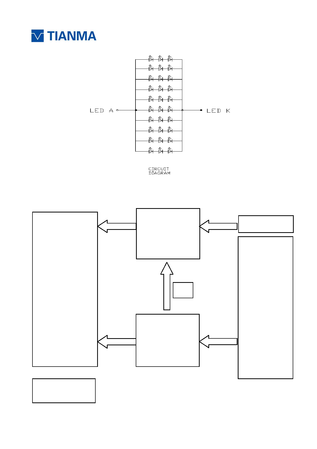
4.3 Block Diagram
VGL
VGH
GatedriverIC
LCDPanel
VCOM
10.1inch
VDD
RESET
1024(RGB)×
STBYB
Rxin0-
600
U/D
Rxin0+
Rxin1-
Rxin1+
Rxin2-
Sourcedriver
Rxin2+
Rxin3-
IC
Rxin3+
+
SELB
AVDD
TCON
L/R
U/D
Backlight
The information contained herein is the exclusive property of TIANMA MICRO-ELECTRONICS Corporation
and shall not be distributed, reproduced, or disclosed in whole or in part without prior written permission of
TIANMA MICRO-ELECTRONICS Corporation.
Page 9 of 42
www.topwaydisplay.com
sales@topwaydisplay.com

+86(755)3699-5528
Shenzhen TOPWAY Technology Co., Ltd.
+86(755)8179-5700
Model No.TM101DDHG04
LED-
LED+
5
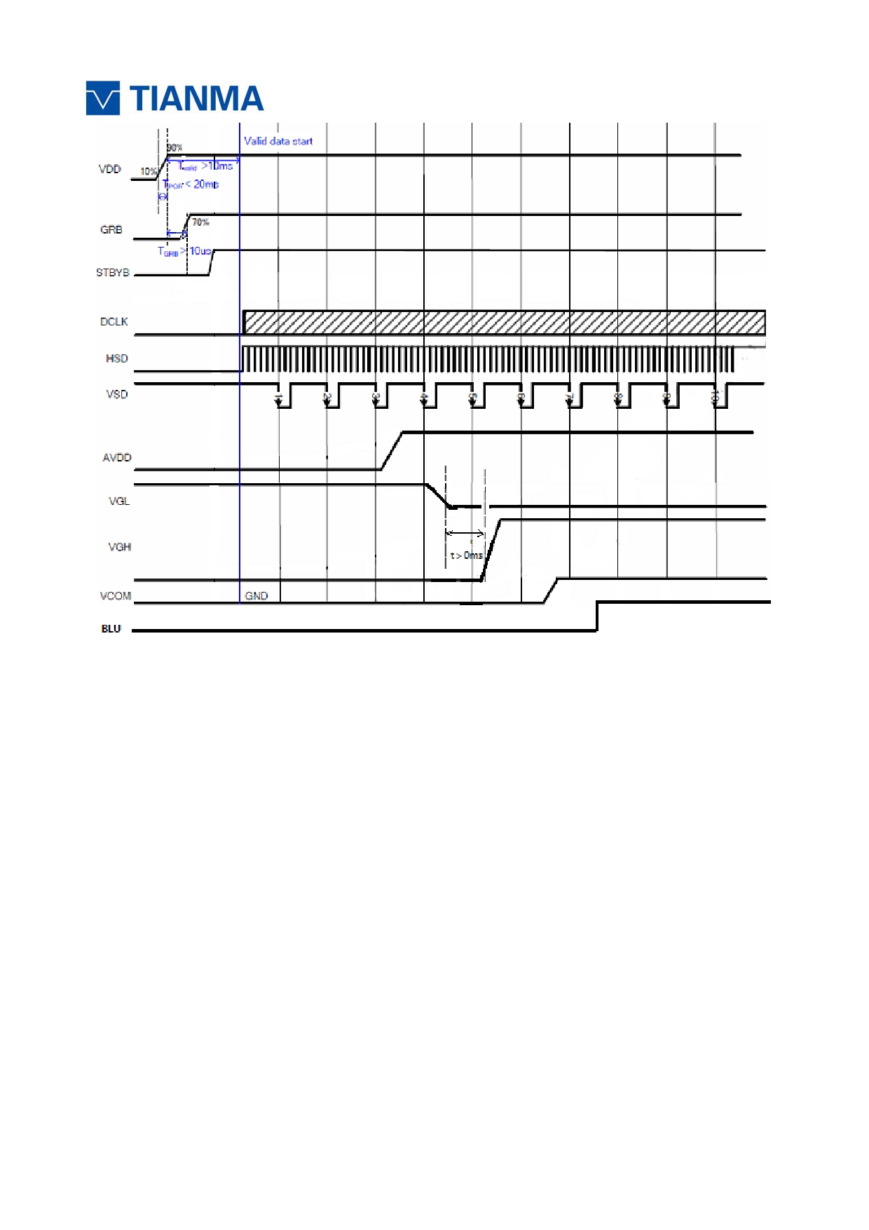
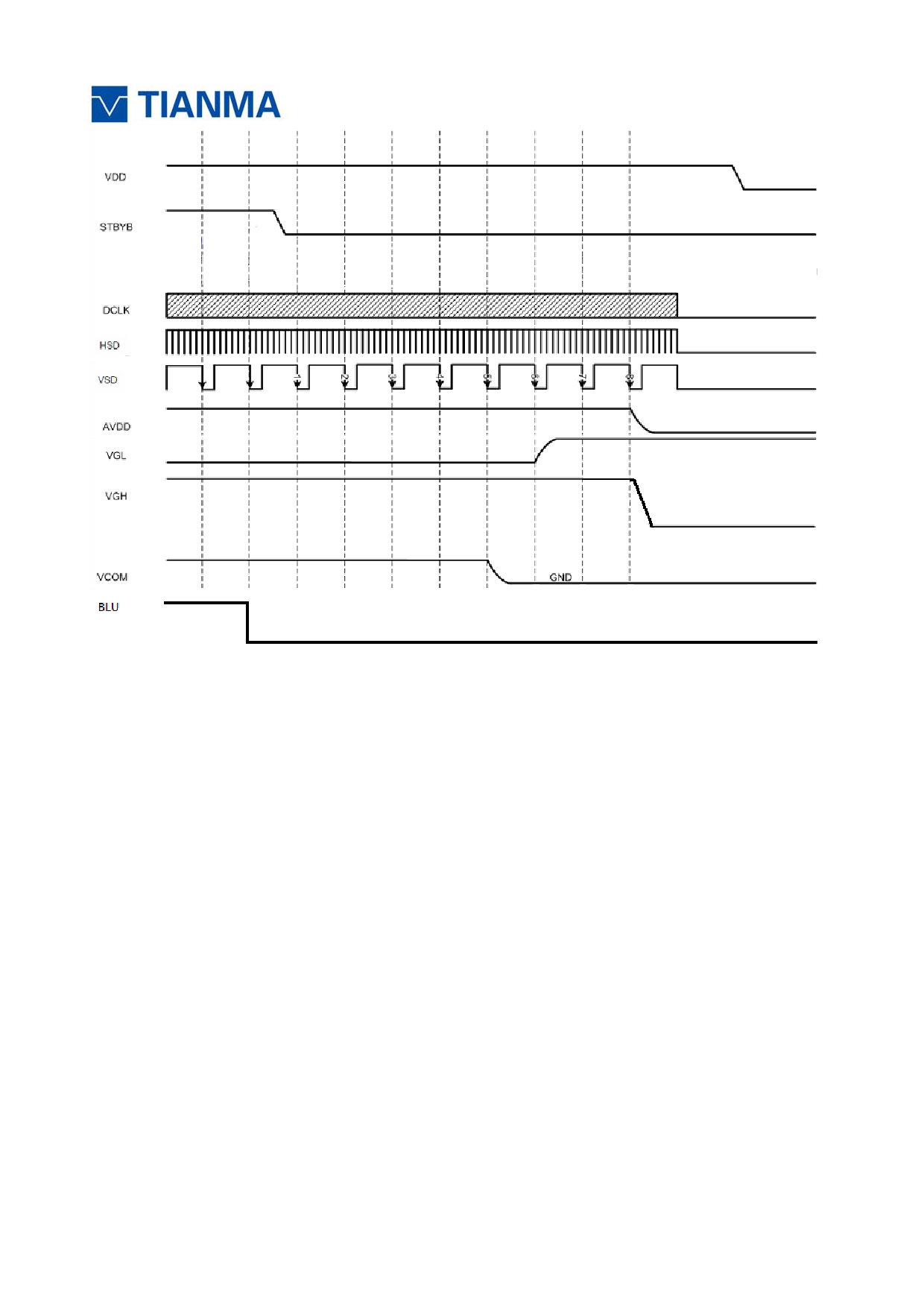
Timing Chart
5.1 Power on/off sequence
The information contained herein is the exclusive property of TIANMA MICRO-ELECTRONICS Corporation
and shall not be distributed, reproduced, or disclosed in whole or in part without prior written permission of
TIANMA MICRO-ELECTRONICS Corporation.
Page 10 of 42
www.topwaydisplay.com
sales@topwaydisplay.com
+86(755)3699-5528
Shenzhen TOPWAY Technology Co., Ltd.
+86(755)8179-5700
Model No.TM101DDHG04
Power on sequence
The information contained herein is the exclusive property of TIANMA MICRO-ELECTRONICS Corporation
and shall not be distributed, reproduced, or disclosed in whole or in part without prior written permission of
TIANMA MICRO-ELECTRONICS Corporation.
Page 11 of 42
www.topwaydisplay.com
sales@topwaydisplay.com
+86(755)3699-5528
Shenzhen TOPWAY Technology Co., Ltd.
+86(755)8179-5700
Model No.TM101DDHG04
Power off sequence
The information contained herein is the exclusive property of TIANMA MICRO-ELECTRONICS Corporation
and shall not be distributed, reproduced, or disclosed in whole or in part without prior written permission of
TIANMA MICRO-ELECTRONICS Corporation.
Page 12 of 42
www.topwaydisplay.com
sales@topwaydisplay.com

+86(755)3699-5528
Shenzhen TOPWAY Technology Co., Ltd.
+86(755)8179-5700
Model No.TM101DDHG04
5.2 LVDS signal timing characteristic
Electrical characteristics
Single-end signals & Differential singals
The information contained herein is the exclusive property of TIANMA MICRO-ELECTRONICS Corporation
and shall not be distributed, reproduced, or disclosed in whole or in part without prior written permission of
TIANMA MICRO-ELECTRONICS Corporation.
Page 13 of 42
www.topwaydisplay.com
sales@topwaydisplay.com
+86(755)3699-5528
Shenzhen TOPWAY Technology Co., Ltd.
+86(755)8179-5700
Model No.TM101DDHG04
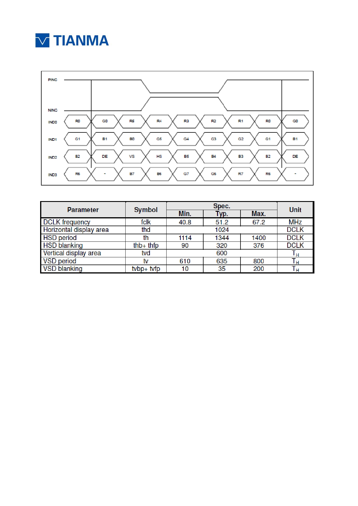
5.3 LVDS mode data input format
8-bit LVDS input Timing
DE mode
The information contained herein is the exclusive property of TIANMA MICRO-ELECTRONICS Corporation
and shall not be distributed, reproduced, or disclosed in whole or in part without prior written permission of
TIANMA MICRO-ELECTRONICS Corporation.
Page 14 of 42
www.topwaydisplay.com
sales@topwaydisplay.com

+86(755)3699-5528
Shenzhen TOPWAY Technology Co., Ltd.
+86(755)8179-5700
Model No.TM101DDHG04
5.4 Display colors and input data signals
This product can display in equivalent to 16,777,216 colors in 256 gray scales. Also the relation
between display colors and input data signals is as the following table.
The information contained herein is the exclusive property of TIANMA MICRO-ELECTRONICS Corporation
and shall not be distributed, reproduced, or disclosed in whole or in part without prior written permission of
TIANMA MICRO-ELECTRONICS Corporation.
Page 15 of 42
www.topwaydisplay.com
sales@topwaydisplay.com
+86(755)3699-5528
Shenzhen TOPWAY Technology Co., Ltd.
+86(755)8179-5700
Model No.TM101DDHG04
6
Optical Characteristics
Item
Symbol Condition
Min
Typ
Max
Unit
Remark
θ T
65
75
-
θ B
70
80
-
View Angles
CR ≧ 10
Degree Note2,3
θ L
70
80
-
θ R
70
80
-
Contrast Ratio
CR
θ =0 o
600
800
-
Note 3
T ON
-
7
10
Response Time
25 ℃
ms
Note 4
T OFF
-
9
18
x
0.241
0.281
0.321
White
Note 1,5
y
0.260
0.300
0.340
x
0.518
0.558
0.598
Red
Note 1,5
y
0.288
0.328
0.368
Chromaticity
Backlight is
x
on
0.276
0.316
0.356
Green
Note 1,5
y
0.522
0.562
0.602
x
0.115
0.155
0.195
Blue
Note 1,5
y
0.074
0.114
0.154
Uniformity
U
70
80
-
%
Note 6
NTSC
40
50
-
%
Note 5
Luminance
L
250
300
-
cd/m 2
Note 7
Test Conditions:
1.
I F = 20 mA, and the ambient temperature is 25 ℃ .
2.
The test systems refer to Note 1 and Note 2.
The information contained herein is the exclusive property of TIANMA MICRO-ELECTRONICS Corporation
and shall not be distributed, reproduced, or disclosed in whole or in part without prior written permission of
TIANMA MICRO-ELECTRONICS Corporation.
Page 16 of 42
www.topwaydisplay.com
sales@topwaydisplay.com
+86(755)3699-5528
Shenzhen TOPWAY Technology Co., Ltd.
+86(755)8179-5700
Model No.TM101DDHG04
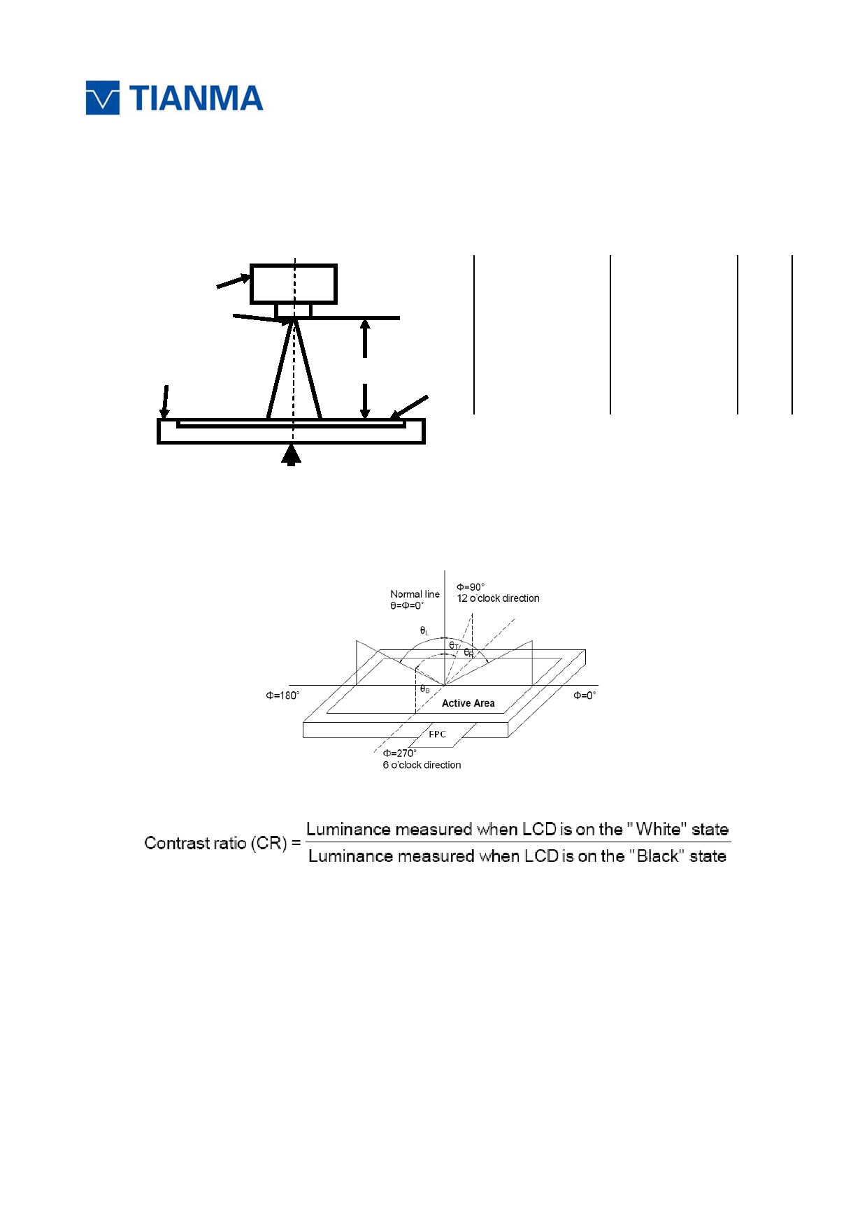
Note 1: Definition of optical measurement system.
The optical characteristics should be measured in dark room. After 5 Minutes operation, the optical
properties are measured at the center point of the LCD screen.
Item
Photo detector
Field
Photo detector
Contrast Ratio
Field
Luminance
SR-3A
1°
Chromaticity
500mm
TFT-LCD Module
Lum Uniformity
LCD Panel
Response Time
BM-7A
2°
The center of the screen
Note 2: Definition of viewing angle range and measurement system.
viewing angle is measured at the center point of the LCD by CONOSCOPE(ergo-80) 。
Note 3: Definition of contrast ratio
“White state “: The state is that the LCD should drive by voltage of white.
“Black state”: The state is that the LCD should drive by voltage of black.
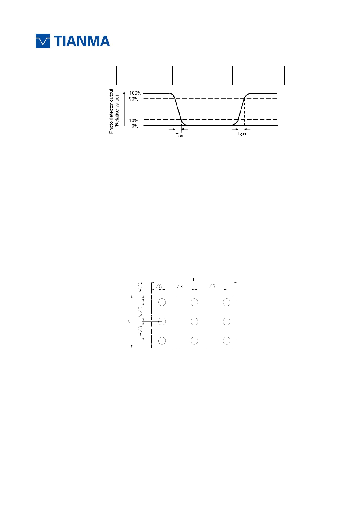
Note 4: Definition of Response time
The response time is defined as the LCD optical switching time interval between “White” state and
“Black” state. Rise time (T ON ) is the time between photo detector output intensity changed from 90%
to 10%. And fall time (T OFF ) is the time between photo detector output intensity changed from 10%
The information contained herein is the exclusive property of TIANMA MICRO-ELECTRONICS Corporation
and shall not be distributed, reproduced, or disclosed in whole or in part without prior written permission of
TIANMA MICRO-ELECTRONICS Corporation.
Page 17 of 42
www.topwaydisplay.com
sales@topwaydisplay.com
+86(755)3699-5528
Shenzhen TOPWAY Technology Co., Ltd.
+86(755)8179-5700
Model No.TM101DDHG04
to 90%.
White (TFT off)
Black (TFT on)
White (TFT off)
Note 5: Definition of color chromaticity (CIE1931)
Color coordinates measured at center point of LCD.
Note 6: Definition of Luminance Uniformity
Active area is divided into 9 measuring areas as below. Every measuring point is placed at the
center of each measuring area.
Luminance Uniformity (U) = Lmin/ Lmax
Lmax: The measured Maximum luminance of all measurement position.
Lmin: The measured Minimum luminance of all measurement position.
L-------Active area length
W----- Active area width
Note 7: Definition of Luminance:
Measure the luminance of white state at center point.
The information contained herein is the exclusive property of TIANMA MICRO-ELECTRONICS Corporation
and shall not be distributed, reproduced, or disclosed in whole or in part without prior written permission of
TIANMA MICRO-ELECTRONICS Corporation.
Page 18 of 42
www.topwaydisplay.com
sales@topwaydisplay.com
+86(755)3699-5528
Shenzhen TOPWAY Technology Co., Ltd.
+86(755)8179-5700
Model No.TM101DDHG04
7
Environmental / Reliability Test
No
Test Item
Condition
Remarks
1
High Temperature
Ta= +50 ℃ ,240hrs
IEC60068-2-1:2007
Operation
GB2423.2-2008
2
Low Temperature
IEC60068-2-1:2007
Operation
Ta= -10 ℃ ,240hrs
GB2423.1-2008
3
High Temperature
IEC60068-2-1:2007
Storage
Ta = +60 ℃ ,240hrs
GB2423.2-2008
4
Low Temperature
IEC60068-2-1:2007
Storage
Ta = -20 ℃ ,240 hrs
GB2423.1-2008
Storage and
5
Operation at high
IEC60068-2-78 :2001
Temperature and
Ta=+60 ℃ , 90% RH 240 hours
GB/T2423.3—2006
Humidity
Start with cold
temperature,
6
Thermal Shock
-20 ℃ 30 min~+60 ℃ 30 min,
End with high
(non-operation)
Change time:5min,100 Cycles
temperature,
IEC60068-2-14:1984,G
B2423.22-2002
MM model : 0 Ω / 200pF ±200 V
7
ESD
IEC61000-4-2:2001
HBM model : 1.5k Ω / 100pF ±1500 V
GB/T17626.2-2006
Stroke:1.5G
8
Vibration Test
Sweep:10Hz~500 Hz
IEC60068-2-6:1982
0.5 hours for each direction of X.Y.Z.
GB/T2423.10—1995
(1.5 hours for total)
9
Mechanical Shock
60G 6ms, ± X,± Y,± Z 3times,
IEC60068-2-27:1987
(Non OP)
for each direction
GB/T2423.5—1995
Note1: Ta is the ambient temperature of sample.
Note2: Before cosmetic and function test, the product must have enough recovery time, at least
2 hours at room temperature.
Note3: In the standard condition, there shall be no practical problem that may affect the display
function. After the reliability test, the product only guarantees operation.
The information contained herein is the exclusive property of TIANMA MICRO-ELECTRONICS Corporation
and shall not be distributed, reproduced, or disclosed in whole or in part without prior written permission of
TIANMA MICRO-ELECTRONICS Corporation.
Page 19 of 42
www.topwaydisplay.com
sales@topwaydisplay.com

+86(755)3699-5528
Shenzhen TOPWAY Technology Co., Ltd.
+86(755)8179-5700
Model No.TM101DDHG04
8
Mechanical Drawing
8.1 Mechanical Drawing
The information contained herein is the exclusive property of TIANMA MICRO-ELECTRONICS Corporation
and shall not be distributed, reproduced, or disclosed in whole or in part without prior written permission of
TIANMA MICRO-ELECTRONICS Corporation.
Page 20 of 42
www.topwaydisplay.com
sales@topwaydisplay.com
+86(755)3699-5528
Shenzhen TOPWAY Technology Co., Ltd.
+86(755)8179-5700
Model No.TM101DDHG04
8.2 FPC Drawing
The information contained herein is the exclusive property of TIANMA MICRO-ELECTRONICS Corporation
and shall not be distributed, reproduced, or disclosed in whole or in part without prior written permission of
TIANMA MICRO-ELECTRONICS Corporation.
Page 21 of 42
www.topwaydisplay.com
sales@topwaydisplay.com
+86(755)3699-5528
Shenzhen TOPWAY Technology Co., Ltd.
+86(755)8179-5700
Model No.TM101DDHG04
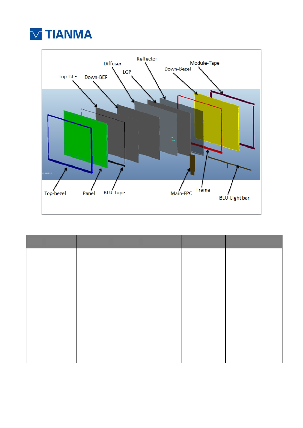
8.3 The Structure of LCM
Part List
NO
Parts
Parts No.
Supplier
Material
Supplier
Parts NO. of Supplier
1
Top Bezel
1610315671
Huiqun
Top Bezel
Huiqun
1610315670
2
Top Pol
1040325450
Sanlipu
Top Pol
Sanlipu
1040325450
3
Bottom pol
1040325460
Sanlipu
Bottom pol
Sanlipu
1040325460
Nippon
Nippon Electric
4
TFT-Glass
1017000170
Electric
TFT-Glass
1100*1300
Glass
Glass
Color
Color
5
F1Y10B050
Inesa
Inesa
T101DSG01T1A
Filter
Filter
Liquid
6
1057000380
HCCH
Liquid crystal
HCCH
HAG635137-A
crystal
Chip
Maxchi
Silicon
7
Source IC
1590322930
HIMAX
Gold bump
ChipMOS
Gold
The information contained herein is the exclusive property of TIANMA MICRO-ELECTRONICS Corporation
and shall not be distributed, reproduced, or disclosed in whole or in part without prior written permission of
TIANMA MICRO-ELECTRONICS Corporation.
Page 22 of 42
www.topwaydisplay.com
sales@topwaydisplay.com

+86(755)3699-5528
Shenzhen TOPWAY Technology Co., Ltd.
+86(755)8179-5700
Model No.TM101DDHG04
NO
Parts
Parts No.
Supplier
Material
Supplier
Parts NO. of Supplier
Chip
UMC
Silicon
8
Gate IC
1590003320
HIMAX
Gold bump
Chipbond
Gold
FPC
Jinpeng
FPC
Housing
Chuguang
URZ2501
Reflector
Tianlihui
UXQ1-100
LGP
Yuanli
PMMA
Diffuser
Jizhi
B100s2
Prism Down
Guangyao
KL77-150
Prism Up
Guangyao
SH26-150
LED
Jufei
CBS206W
Bezel-Down
Dacheng
SUS304
Black-White
double side
Zongyan
SK-8960WB
tape
8
Backlight
1580327041
Weizhi
Double side
Zhongyi
5072
tape
Transparent
Lianchu
LC-100D
PET
Double side
Jishui
550P5BS
tape
Blue release
Zhongyi
Blue release paper
paper
Black-White
Zhongyi
3G-BW650M
side tape
Release film
Zongbang
Z-75140L
Black-Black
double side
Jishui
550MBS
tape
Double side
Tianlihui
3803BH
tape
Solder
Yongan
LF-RMAF8F2
Black ink
Anjiete
70000-00030
The information contained herein is the exclusive property of TIANMA MICRO-ELECTRONICS Corporation
and shall not be distributed, reproduced, or disclosed in whole or in part without prior written permission of
TIANMA MICRO-ELECTRONICS Corporation.
Page 23 of 42
www.topwaydisplay.com
sales@topwaydisplay.com
+86(755)3699-5528
Shenzhen TOPWAY Technology Co., Ltd.
+86(755)8179-5700
Model No.TM101DDHG04
NO
Parts
Parts No.
Supplier
Material
Supplier
Parts NO. of Supplier
9
FOG-ACF
1510000260
Sony
ACF
Sony
CP1220 IS 50M
10
COG-ACF
1510290460
UKC
ACF
UKC
ACF-CP34531-18YA
Base Film
Xinyang
W-1003ED-N2
Protect Film
Taihong
FHT0515
PI
Yaseng
AHIPI820XSS1
Thermosetting
Dongyi
P40-250A1
Adhesive
Ink
Taiyang
S-411W
NI
Xiejin
KG-531
Au
Xiejin
KG-545
RM04FTN6490
Resistance
Dayi
RM04FTN5230
GRM155R61C105KA12D
GRM155R61A105KE15D
Capacitance
Murata
GRM155R61E104KA87D
GRM155R61E105KA12D
11
FPC
1540344300
Sandeguan
CL05A104KP5NNNC
Capacitance
Sumsung
CL05A104KO5NNNC
CL05A225KO5NQNC
RC0402FR-07511RL
RC0402FR-07475RL
RC0402FR-071K02L
RC0402FR-07287RL
RC0402FR-07316RL
RC0402FR-07619RL
RC0402FR-07324RL
Resistance
Guoju
RC0402FR-07590RL
RC0402FR-07390RL
RC0402FR-071K3L
RC0402FR-07143RL
RC0402FR-070RL
RC0402FR-0710KL
RC0402FR-07100RL
RC0402FR-074K7L
IC
Seiko
S-80825CNNB-B8KT2U
Solder
Tamura
TLF-204-NH
The information contained herein is the exclusive property of TIANMA MICRO-ELECTRONICS Corporation
and shall not be distributed, reproduced, or disclosed in whole or in part without prior written permission of
TIANMA MICRO-ELECTRONICS Corporation.
Page 24 of 42
www.topwaydisplay.com
sales@topwaydisplay.com
+86(755)3699-5528
Shenzhen TOPWAY Technology Co., Ltd.
+86(755)8179-5700
Model No.TM101DDHG04
NO
Parts
Parts No.
Supplier
Material
Supplier
Parts NO. of Supplier
12
UV glue
1520000180
Hitachi
UV glue
Hitachi
TF-3348-50F
13
UV glue
1520000120
DYMAX
UV glue
DYMAX
DYMAX-3069-T-moto HF
Tape
Huangguan
7965 7982
14
Tape
1670000940
Juxiang
Red tape
Xianchu
-
Insulation
3M
3M 98C-12
Insulation
Tape
15
1670319790
Hongju
tape
PET
Xianchu
-
Insulation
Insulation
16
1670319860
Renhong
3M
98C-1
tape(Bul)
tape
8.4 Product Code
8.4.1 Bar Code definition on module
Note: Bar Code definition
Definition label is Panel ID, and it is unique and includes manufacture relevant information, for instance
TM101DDHG04. Label definition as below:
M
1
P
6B00400M00 6
B
2 01G
①
②
③
④
⑤ ⑥
⑦ ⑧
① Means shop code A(Array) 、 C(Cell) 、 F(CF) 、 M(Module)
② Means Fab ID 1~9
③ Means Production Type P(production) 、 E(Engineering) 、 D(Dummy) 、 T(Test)
④ Means Lot ID
⑤ Means Years, 0(2010)~9(2019)
⑥ Means Months 1~9,A(Otc) 、 B(Nov) 、 C(Dec)
The information contained herein is the exclusive property of TIANMA MICRO-ELECTRONICS Corporation
and shall not be distributed, reproduced, or disclosed in whole or in part without prior written permission of
TIANMA MICRO-ELECTRONICS Corporation.
Page 25 of 42
www.topwaydisplay.com
sales@topwaydisplay.com

+86(755)3699-5528
Shenzhen TOPWAY Technology Co., Ltd.
+86(755)8179-5700
Model No.TM101DDHG04
⑦ Means Day ….1~31 Day means 1~9 and A~X (Not included I and O)
⑧ Means Serial Number 001~ZZZ (Not included I and O)
8.4.2 Product Name Criterion
TFT Module
Active
Product
Producing
Serial
Serial
Code
Area( size)
Resolution
Type
Area
NO.1
NO.2
T
M
XXX
X
X
H
X
X
X
X
Note: Serial NO.2 will vary as product material change, and serial number manage product
inside of factory.
For Instance: TM:TIANMA
Active Area(size): 3.5inch ---035;10.4inch---104;
Producing Area: H means shanghai Tianma
Resolution
480x240
640x240
960x240
1024x600
128x128
128x160
176x220
240x320
Symbol
A
B
C
D
E
F
G
H
Kind
Delta
Delta
Delta
Stripe
Stripe
Stripe
Stripe
Stripe
Resolution
176x220
1366x800
320x240
240x400
1440x900
400x240
480x234
320x480
Symbol
G
J
K
L
M
N
U
P
Kind
Stripe
Stripe
Stripe
Stripe
Stripe
Stripe
Stripe
Stripe
Resolution
640x480
800x480
800x600
1024x768
others
Symbol
Q
R
S
T
X
Kind
Stripe
Stripe
Stripe
Stripe
--
8.4.3 Product Name Criterion
TSP+BL(CCFL)+FPC+M4
A
TSP+BL(LED)+FPC+M4
B
BL(CCFL)+FPC+M4
C
BL(LED)+FPC+M4
D
BL(LED)+FPC+M4.Dual Display
E
FPC+M4
F
M4
G
M3
H
M2
Y
M1
J
BL(CCFL)+FPC+M4+PCB
K
The information contained herein is the exclusive property of TIANMA MICRO-ELECTRONICS Corporation
and shall not be distributed, reproduced, or disclosed in whole or in part without prior written permission of
TIANMA MICRO-ELECTRONICS Corporation.
Page 26 of 42
www.topwaydisplay.com
sales@topwaydisplay.com

+86(755)3699-5528
Shenzhen TOPWAY Technology Co., Ltd.
+86(755)8179-5700
Model No.TM101DDHG04
BL(LED)+FPC+M4+PCB
L
TSP+BL(CCFL)+FPC+M4+PCB
M
TSP+BL(LED)+FPC+M4+PCB
N
Others
X
M1:Panel(array+CF)
M2:Panel(array+CF+LC)
M3:Panel(array+CF+LC+PLZ)
M4:Panel(array+CF+LC+PLZ+Driver)
Note:
CF: Color Filter, LC: Liquid Crystal, PLZ: Polarization Plate.
8.4.4 Product Manufacture Area
Cell Manufacturer: Shanghai AVIC Optoelectronics Co.,Ltd.
Address: 3388th Huaning Rd.Minhang District,Shanghai.China 201108
Country of Origin: China
Module Manufacturer: ShanghaiTianma Micro-Electronics Co.,Ltd.
Address: 889 huiqing Rd.Pudong District,Shanghai.China 201201
Country of Origin: China
9
Packing Drawing
Unit
No
Item
Model (Material)
Dimensions(mm)
Weight(Kg)
Quantity Remark
1
LCM module
TM101DDHG04
233×137×3.00mm
0.210
36
2
Tray
PET ( Transmit )
485×330×14.00mm
0.150
21
3
Dust-Proof Bag
PE
700×545x0.05mm
0.021
1
4
EPE
EPE
485*330*5mm
0.545
3
5
Box
CORRUGATED PAPER 520*345*74mm
0.227
3
6
Desiccant
DESICCANT
45×35
0.002
6
7
Carton
CORRUGATED PAPER 544*365*250mm
1.01
1
8
Total weight
14.07 ± 5% Kg
The information contained herein is the exclusive property of TIANMA MICRO-ELECTRONICS Corporation
and shall not be distributed, reproduced, or disclosed in whole or in part without prior written permission of
TIANMA MICRO-ELECTRONICS Corporation.
Page 27 of 42
www.topwaydisplay.com
sales@topwaydisplay.com
+86(755)3699-5528
Shenzhen TOPWAY Technology Co., Ltd.
+86(755)8179-5700
Model No.TM101DDHG04
Carton ID
The information contained herein is the exclusive property of TIANMA MICRO-ELECTRONICS Corporation
and shall not be distributed, reproduced, or disclosed in whole or in part without prior written permission of
TIANMA MICRO-ELECTRONICS Corporation.
Page 28 of 42
www.topwaydisplay.com
sales@topwaydisplay.com
+86(755)3699-5528
Shenzhen TOPWAY Technology Co., Ltd.
+86(755)8179-5700
Model No.TM101DDHG04
The information contained herein is the exclusive property of TIANMA MICRO-ELECTRONICS Corporation
and shall not be distributed, reproduced, or disclosed in whole or in part without prior written permission of
TIANMA MICRO-ELECTRONICS Corporation.
Page 29 of 42
www.topwaydisplay.com
sales@topwaydisplay.com

+86(755)3699-5528
Shenzhen TOPWAY Technology Co., Ltd.
+86(755)8179-5700
Model No.TM101DDHG04
10
Precautions for Use of LCD Modules
10.1 Handling Precautions
a. The display panel is made of glass. Do not subject it to a mechanical shock by dropping it from
a high place, etc.
b. If the display panel is damaged and the liquid crystal substance inside it leaks out, be sure not to
get any in your mouth, if the substance comes into contact with your skin or clothes, promptly
wash it off using soap and water.
c. Do not apply excessive force to the display surface or the adjoining areas since this may cause
the color tone to vary.
d. The polarizer covering the display surface of the LCD module is soft and easily scratched. Handle
this polarizer carefully.
e. If the display surface is contaminated, breathe on the surface and gently wipe it with a soft dry
cloth. If still not completely clear, moisten cloth with one of the following solvents:
- Isopropyl alcohol
- Ethyl alcohol
Solvents other than those mentioned above may damage the polarizer. Especially, do not use the
following: - Water
- Ketone
- Aromatic solvents
f. Do not attempt to disassemble the LCD Module.
g. If the logic circuit power is off, do not apply the input signals.
h. To prevent destruction of the elements by static electricity, be careful to maintain an optimum
work environment.
1. Be sure to ground the body when handling the LCD Modules.
2. Tools required for assembly, such as soldering irons, must be properly ground.
3. To reduce the amount of static electricity generated, do not conduct assembly and other work
under dry conditions.
4. The LCD Module is coated with a film to protect the display surface. Be care when peeling off this
protective film since static electricity may be generated.
10.2 Storage precautions
a. When storing the LCD modules, avoid exposure to direct sunlight or to the light of fluorescent
lamps.
b. The LCD modules should be stored under the storage temperature range. If the LCD modules will
be stored for a long time, the recommend condition is:
Temperature : 0 ℃ ~ 40 ℃ Relatively humidity: ≤ 80%
c. The LCD modules should be stored in the room without acid, alkali and harmful gas.
10.3 Transportation Precautions
a. The LCD modules should be no falling and violent shocking during transportation, and also
should avoid excessive press, water, damp and sunshine.
The information contained herein is the exclusive property of TIANMA MICRO-ELECTRONICS Corporation
and shall not be distributed, reproduced, or disclosed in whole or in part without prior written permission of
TIANMA MICRO-ELECTRONICS Corporation.
Page 30 of 42
www.topwaydisplay.com
sales@topwaydisplay.com
+86(755)3699-5528
Shenzhen TOPWAY Technology Co., Ltd.
+86(755)8179-5700
Model No.TM101DDHG04
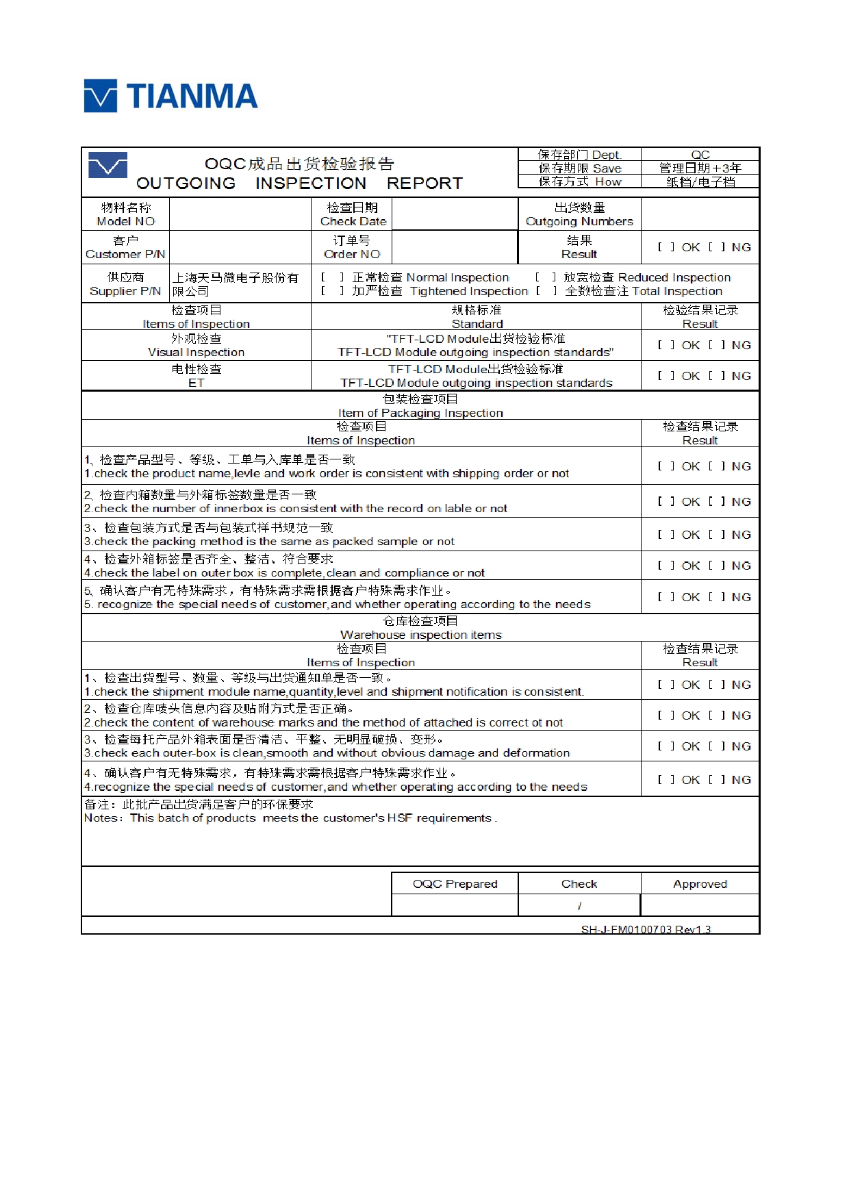
11 Outgoing Inspection Report
Note: This Outgoing Inspection Report what is suitable for all lot of modules is give to customer.
The information contained herein is the exclusive property of TIANMA MICRO-ELECTRONICS Corporation
and shall not be distributed, reproduced, or disclosed in whole or in part without prior written permission of
TIANMA MICRO-ELECTRONICS Corporation.
Page 31 of 42
www.topwaydisplay.com
sales@topwaydisplay.com
+86(755)3699-5528
Shenzhen TOPWAY Technology Co., Ltd.
+86(755)8179-5700
Model No.TM101DDHG04
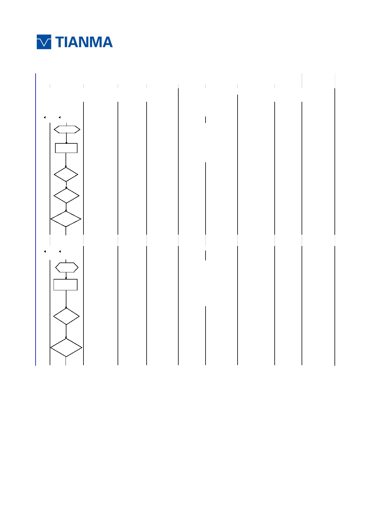
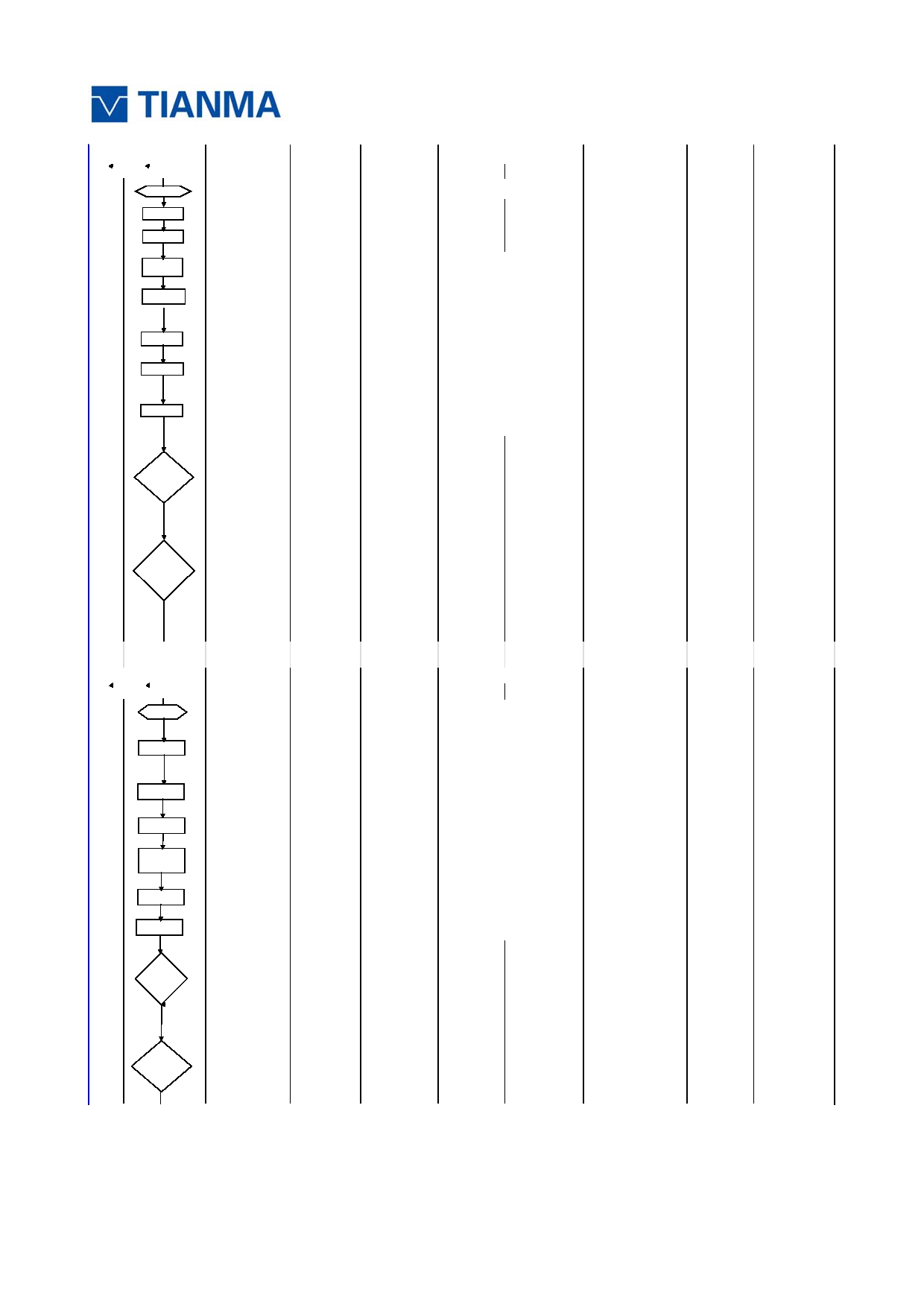
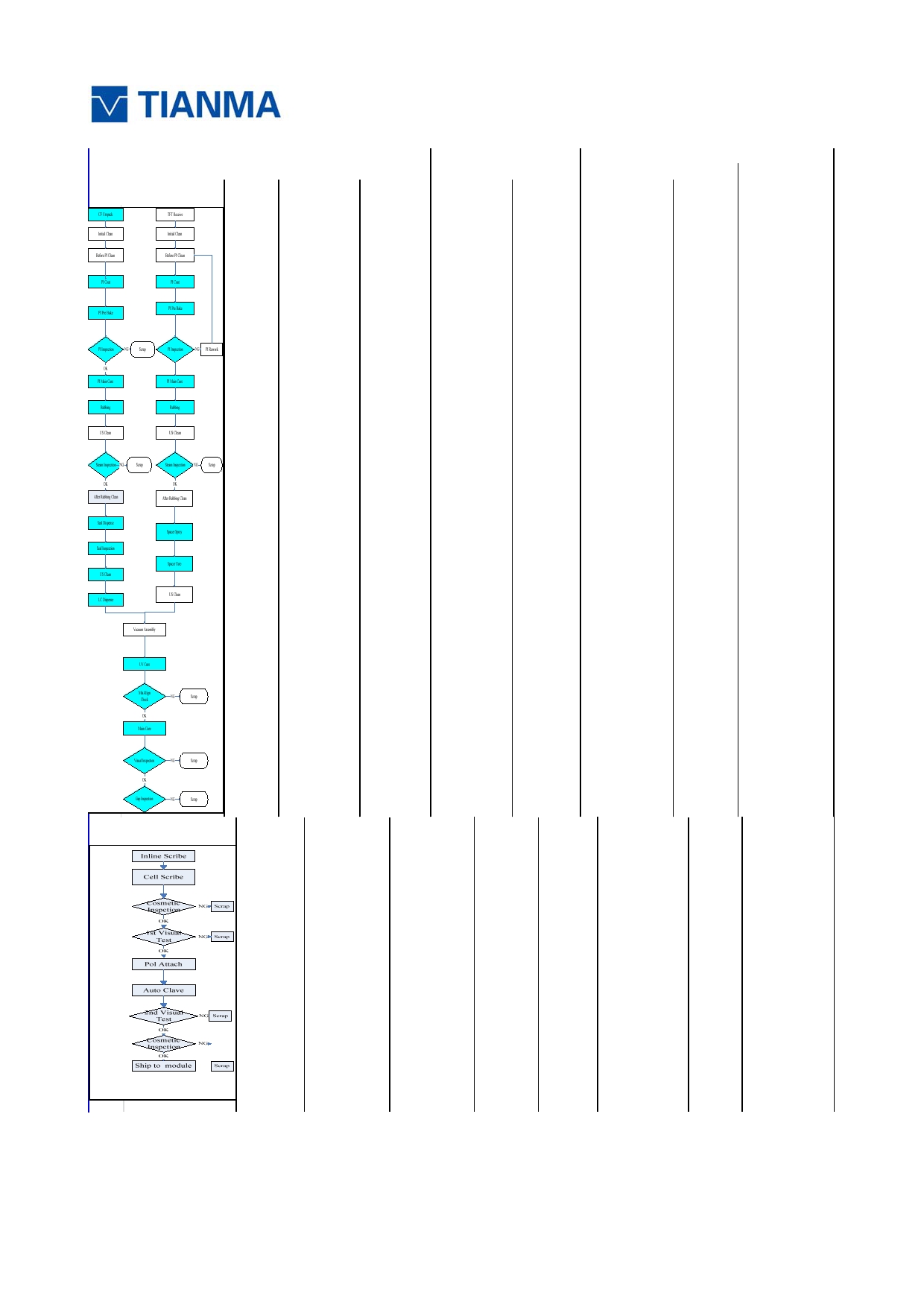
12QC Flow Chart
12.1 Array QC Flow Chart
QC flow chart
Module Name:TM101DDHG03
Revision:1.0
Responsibility:QC
Date(Orig.): 2016-1-04
Date(Rev.):
Prepared by:Zhangheng Xiang
Approved by:Dongjin Song
Measuring
Sample size &frequence
Process
Management Item
Quality Spec
instrument/
Control method
Responsibility
Reaction Plan
Inspection method
LOT ID
SLOT ID
1.EUV lamp(1-4)
all: ON
all
Engineer
pre-depo
Recipe setting
stop production and
by meter
2.Transfer speed
4100-4300 mm/min
all
PQA check
Engineer
Inform shift Enginee
1.discharge pressure
all
2.Ar flow
all
Recipe setting
refer to recipe
PQA check
stop production and
PVD
3.Discharge power
by meter
all
Engineer
card
Inform shift Enginee
4.magnet scan times
all
5.H(0-4) temperature
2次/天
EQ Parameter Check List
S(3-5)temperature
1.Gate:Defect number
1.Gate:Defect≤40
1.Gate:1/2
stop production and
AOI
2.S/D:Defect number
2.S/D:Defect≤30
AOI
2,7
2.S/D: 1/2/3
Recipe setting
Engineer
Inform shift Enginee
PVD
3.ITO:Defect number
3.ITO:Defect≤40
3.ITO: 1/2/3/4
stop production and
1.Gate RS
RS:≤ 0.45±0.07W/□
RSM100
1,6
1.Gate:1/2
Recipe setting
Engineer
Inform shift Enginee
RS
stop production and
2.S/D RS
RS:≤ 0.58±0.2W/□
RSM100
1,6
2.S/D: 1/2/3
Recipe setting
Engineer
Inform shift Enginee
stop production and
3.ITO RS
RS:≤ 85±40W/□
RSM100
1,6
3.ITO: 1/2/3/4
Recipe setting
Engineer
Inform shift Enginee
GATE
Thickness:2600A
stop production and
Thickness
Thickness & uniformity
A1SPR100
1,6
1/12/23
Recipe setting
Engineer
Uniformity:10%
Inform shift Enginee
Sample size &frequence
Measuring
Process
Management Item
Quality Spec
instrument/
Control method
Responsibility
Reaction Plan
Inspection method
LOT ID
SLOT ID
pre-depo
1.EUV lamp(1-4)
all: ON
all
Engineer
Recipe setting
stop production and
cleanning
by meter
PQA check
Inform shift Enginee
2.Transfer speed
4100-4300 mm/min
all
Engineer
Deposition Time
all
Engineer
Gas ingredient
all
Engineer
CVD
Pressure
refer to Array
all
Recipe setting
Engineer
stop production and
by meter
recipe card
PQA check
Inform shift Enginee
Space
all
Engineer
R/F power
all
Engineer
Chamber Temperature
all
Engineer
stop production and
CVD
1.Active:Defect number 1.Active:Defect≤30
2,7
1/2
Engineer
AOI
Inform shift Enginee
AOI
Recipe setting
2.Passivation:Defect
2.Passivation:
stop production and
2,7
1/2
Engineer
number
Defect≤30
Inform shift Enginee
Thickness:
SiNx 3000 ±300A
1.Active:
A1ELL100
stop production and
a-Si 2000 ±200A
1/2/3
Engineer
Thickness & uniformity
A1SPR100
Inform shift Enginee
n+ a-Si 500 ±50A
Thickness
Uniformity:≤ ±10%
1,6
Recipe setting
measure
Thickness:
2.Passivation:Thickness
stop production and
P-SiNx 2000 ±200A
A1SPR100
1/2/3
Engineer
& uniformity
Inform shift Enginee
Uniformity:≤ ±10%
The information contained herein is the exclusive property of TIANMA MICRO-ELECTRONICS Corporation
and shall not be distributed, reproduced, or disclosed in whole or in part without prior written permission of
TIANMA MICRO-ELECTRONICS Corporation.
Page 32 of 42
www.topwaydisplay.com
sales@topwaydisplay.com
+86(755)3699-5528
Shenzhen TOPWAY Technology Co., Ltd.
+86(755)8179-5700
Model No.TM101DDHG04
Measuring
Sample size &frequence
Process
Management Item
Quality Spec
instrument/
Control method
Responsibility
Reaction Plan
Inspection method
LOT ID
SLOT ID
Cleanning
EUV illuminance
≥40mw/cm2,Uni.<15%
TEL CS1000
1/week
《Euv intensity measurement》
Engineer
adjust the recipe
Bake
Cooling
PR Coating
1.5±0.05um,
TPR
SR
1/2weeks
《TPR Trend Chart》
Engineer
adjust the recipe
Uni.±4%
VCD Parameter
all
Recipe setting
Engineer
stop machine
Bake
Recipe setting
SB Parameter
refer to Array
TEL CS1000
all
Engineer
test more and rework
recipe card
PQA check
Recipe setting
HB Parameter
all
Engineer
test more and rework
PQA check
Cooling
Scan speed
MPA6000
all
Recipe setting
Engineer
adjust the recipe
refer to Array
Exposure
exposure illuminance
1/week
recipe card
MPA6000
《MPA Intensity Uni.》
Engineer
adjust the recipe
Step Parameter
MPA6000
all
Recipe setting
Engineer
adjust the recipe
Development Temperature
23±0.5℃
TEMP MONITOR
1/Shift
《EQ Parameter Check List》
Engineer
stop machine
Developer concentration
2.380±0.01%
NAGAS MONITOR
1/Shift
《EQ Parameter Check List》
Engineer
stop machine
PHOTO
Develop
Developer flow
13L/min,+3/-4
NAGAS MONITOR
1/Shift
《EQ Parameter Check List》
Engineer
adjust the recipe
refer to Array
Recipe setting
Developer time
TEL CS1000
all
Engineer
test more and rework
recipe card
PQA check
1.Gate:Defect≤40
1/2/23
daily Process Chart
Engineer
test more and rework
2.Active:Defect≤30
1/2/23
daily Process Chart
Engineer
test more and rework
1. Initial
Defect number
3.S/D;Defect≤30
A1ADI300 (100/400) workpiece Confirm
1/2/23
daily Process Chart
Engineer
test more and rework
ADI
4.Passivation:
2. 2,7
1/2/23
daily Process Chart
Engineer
test more and rework
Defect≤30
5.ITO:Defect≤40
1/2/23
daily Process Chart
Engineer
test more and rework
1.Initial
rework and adjust the
CD:±0.5um
workpiece Confirm
1/2/23
SPC
Engineer
recipe
2. 1
1.Initial
rework and adjust the
CD bar:±0.5um
workpiece Confirm
1/2/23
SPC
Engineer
recipe
2. 1
1.Initial
CD bar:±0.5um
rework and adjust the
CD
workpiece Confirm
1/2/23
SPC
Engineer
Overlay:<1.2um
recipe
Measure
CDC&OL
A1CDC100
2. 1
1.Initial
Via:±0.5um
rework and adjust the
workpiece Confirm
1/2/23
SPC
Engineer
Overlay:<1.2um
recipe
2. 1
1.Initial
CD bar: ±0.5um
rework and adjust the
workpiece Confirm
1/2/23
SPC
Engineer
Overlay:<1.2um
recipe
2. 1
Sample size &frequence
Process
Management Item
Quality Spec
Measuring
instrument/
Control method
Responsibility
Reaction Plan
Inspection method
LOT ID
SLOT ID
EUV
EUV illuminance
>40mw/cm2
by meter
1/shift
《EQ Parameter Check List》
Engineer
Inform shift Enginee
refer to Array
Recipe setting
Etch time
by meter
all
Engineer
recipe card
PQA check
Etching
refer to Array
TANK temperature
by meter
1/shift
《EQ Parameter Check List》
Engineer
recipe card
Inform shift Enginee
refer to Array
Chemical concentration
by EMS
1/shift
《EQ Parameter Check List》
Engineer
recipe card
Rinse
refer to Array
Spray Flow
by meter
all
《EQ Parameter Check List》
Engineer
Inform shift Enginee
recipe card
refer to Array
Air.Knife
A.Knife flow
by meter
1次/shift
《EQ Parameter Check List》
Engineer
Inform shift Enginee
recipe card
refer to Array
Recipe setting
Oscillation Time
by meter
all
Engineer
Inform shift Enginee
Stripper
recipe card
PQA check
refer to Array
Recipe setting
Tank temperature
by meter
1/shift
Engineer
Inform shift Enginee
recipe card
PQA check
refer to Array
Rinse
Spray Flow
by meter
1/shift
《EQ Parameter Check List》
Engineer
Inform shift Enginee
WET
recipe card
refer to Array
Air.Knife
A.Knife flow
by meter
1/shift
《EQ Parameter Check List》
Engineer
Inform shift Enginee
recipe card
1.Initial
1.Gate:Defect number
1.Gate:Defect≤40
workpiece Confirm Gate:1/12/23
Engineer
Inform shift Enginee
2. 2,7
1.Initial
AEI
2.S/D:Defect number
2.S/D:Defect≤30
A1AEI300 (100/200) workpiece Confirm S/D: 1/12/23
Recipe setting
Engineer
Inform shift Enginee
2. 2,7
1.Initial
3.ITO:Defect number
3.ITO:Defect≤40
workpiece Confirm ITO: 1/12/23
Engineer
Inform shift Enginee
2. 2,7
1.Gate CD
CD:±0.5um
2.CD
CD bar:±0.5um
1.Initial
CDC
A1CDC200
workpiece Confirm
1/12/23
Recipe setting
Engineer
Inform shift Enginee
Measure
3.S/D CD
CD:±0.5um
2. 2,7
4.ITO CD
CD bar:±0.5um
The information contained herein is the exclusive property of TIANMA MICRO-ELECTRONICS Corporation
and shall not be distributed, reproduced, or disclosed in whole or in part without prior written permission of
TIANMA MICRO-ELECTRONICS Corporation.
Page 33 of 42
www.topwaydisplay.com
sales@topwaydisplay.com
+86(755)3699-5528
Shenzhen TOPWAY Technology Co., Ltd.
+86(755)8179-5700
Model No.TM101DDHG04
12.2 Cell QC Flow Chart
Module Name:TM101DDHG03
Revision:1.0
Responsibility:QC
Date(Orig.): 2016-1-04
Date(Rev.):
Prepared by:Zhangheng Xiang
Approved by:Dongjin
Song
Measuring
process
Sample size
process name Management Item
Quality Spec
instrument/
&frequence
Control Method
Responsibility
Reaction Plan
Inspection method
1.CF corner direction
1.Upleft
OIC auto inspection
CF unpack
100%
EQ alram automatic
Engineer
Inform Engineer and IQC
2.Vacuum Error
2.>-50Kpa
+visual inspection
1.Thickness
1.1000±100Å
1.By Array SPR
1.2Sheet/week
Inspect All Sheet and Inform
PI Coat
Process Card
Engineer
2.printing accuracy
2.±0.3mm
2.CCD visual insp
2.1S/line change
Engineer
1.Precure Temperature
1.100℃±3°C
Inspect All Sheet and Inform
PI Pre Bake
EQ Setting
First Lot 1sheet/Lot
Process Card
Engineer
2.Precure Time
2.120sec
Engineer
1.CELL inspection
Inspect All Sheet and Inform
PI inspection
1.printing quality
AOI inspectiong
100%
《PI Ispection record List》
Operator
standards
Engineer
1.MainCure Temperature
1.230°C±5℃
Inspect All Sheet and Inform
PI Main Bake
2.MainCure Time
2.1800sec
EQ Setting
First Lot 1sheet/Lot
Process Card
Operator
Engineer
3.Cooling Time
3.360sec
Inspect All Sheet and Inform
Rubbing
ODF Cell Gap Instrument
SPC control
Engineer
1.Pretilt angle
1.Process card
1.2sheet/LOT
Engineer
1.Film appearance
《Rubbing Ispectionrecord
Steam Inspection
1.No Defect
1.Steam inspection
1.1sheet/LOT
Engineer
product hold,inform Engineer
List》
1.First Piece Check
1.Seal Area Accuracy
1.Process card
1.1sheet/10sheet
《Seal dispensor condition
product continuous and
2.N2 pressure
1.By Laser Sensor
Seal Dispence
2.0.45Mpa±0.15Mpa
2.confirm when line
adjust record sheet》
Engineer
restart after adjust to
3.coating speed
2.EQ Setting
3.80mm/s
change
2.《ODF lint start/change
normal
check sheet》
1.Spacer density
1.220±25ea/mm2
2.Spray Accuracy
1.Spcaer Counter
1.All inspect by EQ
2.CV < 15%
1.100%
product continuous and
Spacer Spray
3.Cluster Counter
2.OP confirm recipe
2.《ODF line start/change
OP
3.L<10;M<20;S<40
2.1sheet(First Lot)
restart after adjust to norma
4.Density inspection
setting when line change
check sheet》
4.20个
point number
1.EQ auto inspection
1.Cure Temperature
1.120±3℃
《ODF line start/change
product continuous,and EQ
Spcer Cure
2.OP confirm recipe
First Lot
OP
2.Cure Time
2.600Sec
check sheet》
stop,inform engineer
setting when line change
1.4.0±0.2um
1. 2 sheet/LOT
1. SPC control
1.Gap Measurement
2.Process card
1.Cell Gap
2.check at line
2.《ODF lint start/change
2.LC drop amount
Inform Engineer to confirm EQ
LC Dispence
3.Auto adjust to±
2.Recipe Setting
change
check sheet》
Engineer/OP
3.LC drop accuracy
status
0.3% when production 3.EQ auto measure
3.Process
3.EQ auto sampling,and
4.LC type
4.Process card
20sheet/time
record
1.Lighting Illumination 1.160mw/cm
《ODF lint start/change
Product hold, inform engineer
UV Cure
Recipe Setting
First Lot/1Time
Engineer
2.UV Lighting Time
2.50Sec
check sheet》
confirm EQ status
MisAlign
Vacuum Assembly System &
Product hold, inform engineer
±5μm
Misalign checker
5sheet/lot
SPC control
Engineer
inspection
Misalign Checker
confirm EQ status
1.Cure Temperature
1.120±3℃
《ODF lint start/change
Product hold, inform engineer
Main Cure
EQ auto check
First Lot/1Time
Engineer
2.Cure Time
2.3600Sec
check sheet》
confirm EQ status
1.LC divulge
Visual
Product hold, inform engineer
2.display abnormal
1.No
visual inspectiong
100%
inspectiong record
Operator
Inspection
confirm EQ status
3.LC bubble
Product hold, inform engineer
Gap Inspection
cell gap
Process card
EQ auto measure
2sheet/lot
SPC control
Engineer
confirm EQ status
Measuring
process
Sample size
Responsibil
process name
Management Item
Quality Spec
instrument/
&frequence
Control Method
ity
Reaction Plan
Inspection
Q/S4001-2008 Cell 1/4
Hold Products,Stop
Inline Scribe
1.Panel Appearance
outgoing inspection
Visual Check
100%
Process Flow List
Operator
Producing
standards
Inform Engineer
innitial workpiece
Hold Products,Stop
CELL Scribe
1.Cutting Precision
1.±0.15mm/Recipe Card 1.AOI
1pcs/machine
confirm/switch mode
OP/Engineer
Producing
Inform Engineer
1.Q/S-4007-2008
Hold Products,Stop
Cosmetic
1.Panel Appearance
TFT-LCD Cell outgoing
Visual Check
100%
Process Flow List
Operator
Producing
Inspection
inspection standards
Inform Engineer
1.Q/S-4007-2008
Hold Products,Stop
1ST V/T
1.display quality
TFT-LCD Cell outgoing
Jig
100%
1.1ST V/T yield data
Operator
Producing
inspection standards
Inform Engineer
1.Pol Attach Position
Accuracy
1.Recipe Card
1.first lot check
Hold Products,Stop
2. Particle
2.Q/S-4007-2008
Pol Attach
2.Jig
8PCS/LOT
POL attach check record
Operator
Producing
3. VM1
TFT-LCD Cell outgoing
3. Visual Check
Inform Engineer
4.Black gap
inspection standards
5.Broken
1.temp
Hold Products,Stop
Auto Clave
2.pressure
1.Recipe Card
Parameter Check
1.1 time/class
Process Flow List
Operator
Producing
3.time
Inform Engineer
Q/S-4007-2008
Hold Products,Stop
2nd V/T
1.display quality
TFT-LCD Cell outgoing
Jig
100%
2ST V/T yield data
Operator
Producing
inspection standards
Inform Engineer
Q/S-4007-2008
Hold Products,Stop
Cosmetic
1.Appearance quality
TFT-LCD Cell outgoing
Visual Check
100%
Cosmetic yield data
Operator
Producing
Inspection
inspection standards
Inform Engineer
The information contained herein is the exclusive property of TIANMA MICRO-ELECTRONICS Corporation
and shall not be distributed, reproduced, or disclosed in whole or in part without prior written permission of
TIANMA MICRO-ELECTRONICS Corporation.
Page 34 of 42
www.topwaydisplay.com
sales@topwaydisplay.com

+86(755)3699-5528
Shenzhen TOPWAY Technology Co., Ltd.
+86(755)8179-5700
Model No.TM101DDHG04
12.3 Module QC Flow Chart
Module Name:TM101DDHG03
Revision:1.0
Responsibility:QC
Date(Orig.): 2016-1-04
Date(Rev.):
Prepared by:Zhangheng Xiang
Approved by:Dongjin Song
Measuring instrument/
Process
Sample size
Process name
Management Item
Quality Spec
Inspection method
Responsibil
&frequence
Control method
Reaction Plan
ity
1.Panel cleanliness 1.water angle≤15°
2.Time
2.process card
《COG switch line list》
1.inform engineer
COG
1.water angle instrument
innitial workpiece
Operator
COG bonding
3.Pressure
3.process card&COG profile
《Module COG Bonding list
2.adjust and confirm
2/3/4.COG insrument
confirm/switch mode
PQC
4.Temperature
4.process card&COG profile
》
sample again
5.FUJI paper
5.Parallelism
5.pressure standard
1.ACF Bonding effect
1. confirm again
AOI
AOI
2.IC bonding
1.Moudle test standard
Microscope
100%
Machine alarm
Operator
2.adjust and confirm
accuracy
sample again
1.check pre and post20
1.Temp
pieces
ACF
2.Pressure
《J-FM0101402 MODULE FOG
2.if find more than one
ACF
3.Time
1.Thermometer Record/Check
1.Microscope
First Piece Check
Operator
ACF List》
defective
products,inform
engineer
1.Attachment State
1.Load Cell Pressure
1.process card&FOG profile
《MODULE FOG BONDING list
2.Parallelism
Tester/EQ Parameter
2.pressure standard
》
1.inform engineer
FOG
2.FUJI paper
innitial workpiece
FOG
3.Temperature
3.process card&FOG profile
《FOG pressure list》
Operator
2.adjust and confirm
4.Time
3、4.Temp. Tester/EQ
confirm/switch mode
4.process card
《Pull test list》
sample again
5,FPC pulling force 5.above 0.6N/mm
Parameter
5.Pull Tester
1.check pre and post20
1.FOG Bonding effect
《Module COG BONDING list
pieces
MI
10%
》
2.if find more than one
MI
2.IC bonding
1.Moudle test standard
1.Microscope
Operator
accuracy
《LCM MI Record》
defective
2.SPC control
《Module SPC list》
products,inform
engineer
1.innitial workpiece
Glue
1.Glue code
confirm
《MODULE glue coating list
1.appearance
Glue coating&UV
1/2.process card&SOP
2.1 time/shift
》
Operator
1.adjust/check and
coating&U cure
2.UV energe
2.UV tester
3.RIF appearance
3.process card
3.innitial workpiece
《equipment maintian list PQC
inform engineer
3.callipers
confirm:6piece/lot
》
V cure
10pieces/2hours
1.Initial workpiece
1.Test tool
1.pross card
Confirm: 6pieces/1
1.ET tool
《 Electrical Property
ET1
2.Display quaility
2、3《TFT-LCD Moudle test
time/1 lot
1.adjust/check and
ET1
3.Light intensity
2.electrical test
list》
Operator
standard》
2.all lot
inform engineer
3.illuminometer
《Light intensity list》
3.1 time/1month
BL
1.innitial workpiece
1.adjust/check and
Assembly
BL Assembly
assembly quality
process card&SOP
visual check
confirm:6piece/lot
《MODULE ASSY List》
Operator
inform engineer
2.all lot
Bezel
1.Bezel Model
1.innitial workpiece
Assembly
1.adjust/check and
Bezel Assembly 2.Bezel Assembly
1/2.process card&SOP
visual check
confirm:6piece/lot
《MODULE ASSY List》
Operator
State
inform engineer
2.all lot
Tape
1.innitial workpiece
1.adjust/check and
Affixed
Tape Affixed
attaching quality
process card&SOP
visual check
confirm:6piece/lot
《MODULE ASSY List》
Operator
inform engineer
2.all lot
1.Initial workpiece
1.Test tool
1.pross card
Confirm: 6pieces/1
1.ET tool
《 Electrical defect
2.Display quality
2、3《TFT-LCD Moudle test
time/1 lot
1.adjust/check and
ET2
ET2
2.electrical test
property list》
Operator
3.Light intensity
standard》
2.all lot
inform engineer
3.illuminometer
《Light intensity list》
3.spot check:1
time/1month
1.Initial workpiece
Cosmetic
1.pross card
Confirm: 6pieces/1
《Visual defect property
inspection
Cosmetic
1.Appearance quality 2.《TFT-LCD Moudle test
time/1 lot
1.adjust/check and
1.visual test
list》
Operator
Inspection
2.Light intensity
standard》
2.all lot
inform engineer
2.illuminometer
《Light intensity list》
3.spot check:1
time/1month
1.Test tool
1.pross card
1.ET/VT tool
OQC
2.Display quality
1.AQL:0.25
2、3、4《TFT-LCD Moudle test
2.electrical test
《OQC inspection list》
OQC
3.Appearance quality standard》
2.1 time/1 month
OQC
goods rejected
3.visual test
《Light intensity list》
4.Light intensity
4.illuminometer
1.packing method
1/2.Initial workpiece
1.pross card
Operator
adjust and confirm
Packing
package
2.packing quality
1.visual check
Confirm: 6pieces/1
《 MODULE packing list 》
2.process card&SOP&BOM
sample again
time/1 lot
The information contained herein is the exclusive property of TIANMA MICRO-ELECTRONICS Corporation
and shall not be distributed, reproduced, or disclosed in whole or in part without prior written permission of
TIANMA MICRO-ELECTRONICS Corporation.
Page 35 of 42
www.topwaydisplay.com
sales@topwaydisplay.com
+86(755)3699-5528
Shenzhen TOPWAY Technology Co., Ltd.
+86(755)8179-5700
Model No.TM101DDHG04
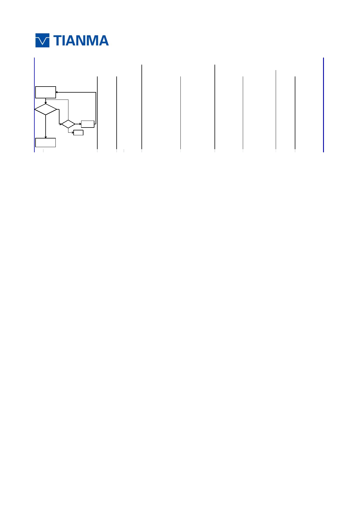
12.4 Rework QC Flow Chart
QC flow chart
TM101DDHG04-00
Revision:1.0
Responsibility:QC
Date(Orig.):
Date(Rev.):
Prepared by:Zhangheng Xiang
Approved by:Dongjin Song
Measuring instrument/
Process
Sample size
Process name
Management Item
Quality Spec
Inspection method
&frequence
Control method
Responsibil
Reaction Plan
ity
Process 1
NG
Check
OK
OK
1.Bonding effect
(CFOG FA)
1.Microscope
《SH-H-FM0121803 Module
1.process card
1. confirm again
FA
Disassemble
2.Bonding accuracy
2.ET/VT tool
rework list》
Operator
Rework
2.rework SOP
100%
2.adjust and confirm
Repair
(CFOG FA)
3.Visual test
《SH-H-FM0121804 Module FA
PQC
3.moudle test standard
sample again
NG
3.Assemble quality
4.Bakelite solid bars
list》
Scrap
4.Welding quality
Process 2
The information contained herein is the exclusive property of TIANMA MICRO-ELECTRONICS Corporation
and shall not be distributed, reproduced, or disclosed in whole or in part without prior written permission of
TIANMA MICRO-ELECTRONICS Corporation.
Page 36 of 42
www.topwaydisplay.com
sales@topwaydisplay.com

+86(755)3699-5528
Shenzhen TOPWAY Technology Co., Ltd.
+86(755)8179-5700
Model No.TM101DDHG04
13 Incoming Inspection Standard
13.1. Scope:
The incoming inspection standards shall be applied to TFT-LCD Modules (hereinafter called
"Modules") that supplied by Shanghai Tianma Micro-Electronics Corporation.
13.2. Incoming Inspection
The customer shall inspect the modules within twenty calendar days of the delivery date ( the
“inspection period ) at its own cost. The result of the inspection ( acceptance or
rejection ) shall be
recorded in writing, and a copy of this writing will be promptly sent to the seller, If the results of the
inspecting from buyer does not send to the seller within twenty calendar days of the delivery date.
The modules shall be regards as acceptance.
Should the customer fail to notify the seller within the inspection period, the buyers right to reject the
modules. Shall be lapsed and the modules shall be deemed to have been accepted by the buyer.
13.3. Inspection Sampling Method
13.1. Lot size: Quantity per shipment lot per model
13.2. Sampling type: Normal inspection, Single sampling
13.3. Inspection level:
Please see the detail information as below:
Lot Size
Cosmetic Check
Function Check
Dimension Check
Ac:Re
Ac:Re
(Minor
N
n
(Major
n
Ac:Re
n
Ac:Re
defects
defects)
)
2~500
50
1:2
501~1200
75
1201~3200
120
3201~10000
0:1
5
0:1
5
0:1
10001~35000
135
2:3
35001~150000
170
150001~500000
200
≥500001
245
Notes :
Cosmetic check :
Cosmetic defects are classified as major defects and minor defects according to the degree of
defectiveness.
The information contained herein is the exclusive property of TIANMA MICRO-ELECTRONICS Corporation
and shall not be distributed, reproduced, or disclosed in whole or in part without prior written permission of
TIANMA MICRO-ELECTRONICS Corporation.
Page 37 of 42
www.topwaydisplay.com
sales@topwaydisplay.com
+86(755)3699-5528
Shenzhen TOPWAY Technology Co., Ltd.
+86(755)8179-5700
Model No.TM101DDHG04
Item No
Items to be inspected
Missing function
missing
Major defects
component
Crack
Glass Crack
Obvious cosmetic defect ,
1 ) Protective film broken
Minor defects
but do not influence
2 ) Pol scratch
product' finally using
Function check :
Item No
Items to be inspected
1) No display
2) Display abnormally
Function defect
Function
3) Short circuit
4) line defect
Dimension check :
Item No
Items to be inspected
Important product‘s size which may influence costumer
Dimension
side assembly
13.4. Inspection Conditions
13.4.1 Ambient conditions:
a. Temperature: Room temperature 25±5 ℃
b. Humidity: (60±10) % RH
c. Illumination: Appearance 700±100 Lux, Display 100±50 Lux (The luminance at an inspection
desk surface with single non-directive fluorescent lamp)
13.4.2 Viewing distance
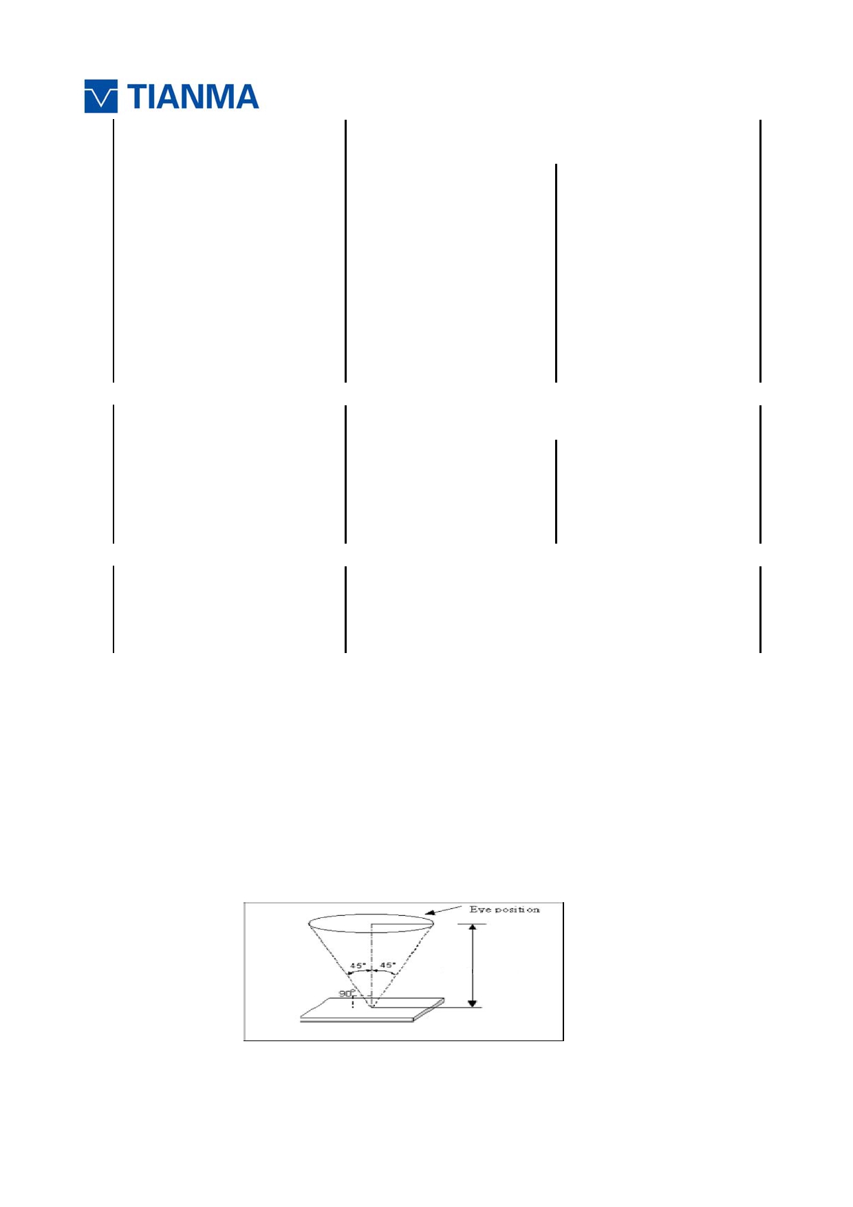
The distance between the LCD and the inspector’s eyes shall be at least 30±5 ㎝ .
13.4.3 Viewing Angle
U/D: 45º/45º, L/R: 45º/45º
The information contained herein is the exclusive property of TIANMA MICRO-ELECTRONICS Corporation
and shall not be distributed, reproduced, or disclosed in whole or in part without prior written permission of
TIANMA MICRO-ELECTRONICS Corporation.
Page 38 of 42
www.topwaydisplay.com
sales@topwaydisplay.com
+86(755)3699-5528
Shenzhen TOPWAY Technology Co., Ltd.
+86(755)8179-5700
Model No.TM101DDHG04
13.5. Inspection Criteria
Defects are classified as major defects and minor defects according to the degree of defectiveness
defined herein.
13.5.1 Major defect
Item No
Items to be
inspected
Inspection Standard
All functional
1) No display
a
defects
2) Display abnormally
3) Short circuit
4) line defect
b
missing
Missing function component
c
Crack
Glass Crack
13.5.2 Minor defect
Item
Items to be
No
inspected
Inspection standard
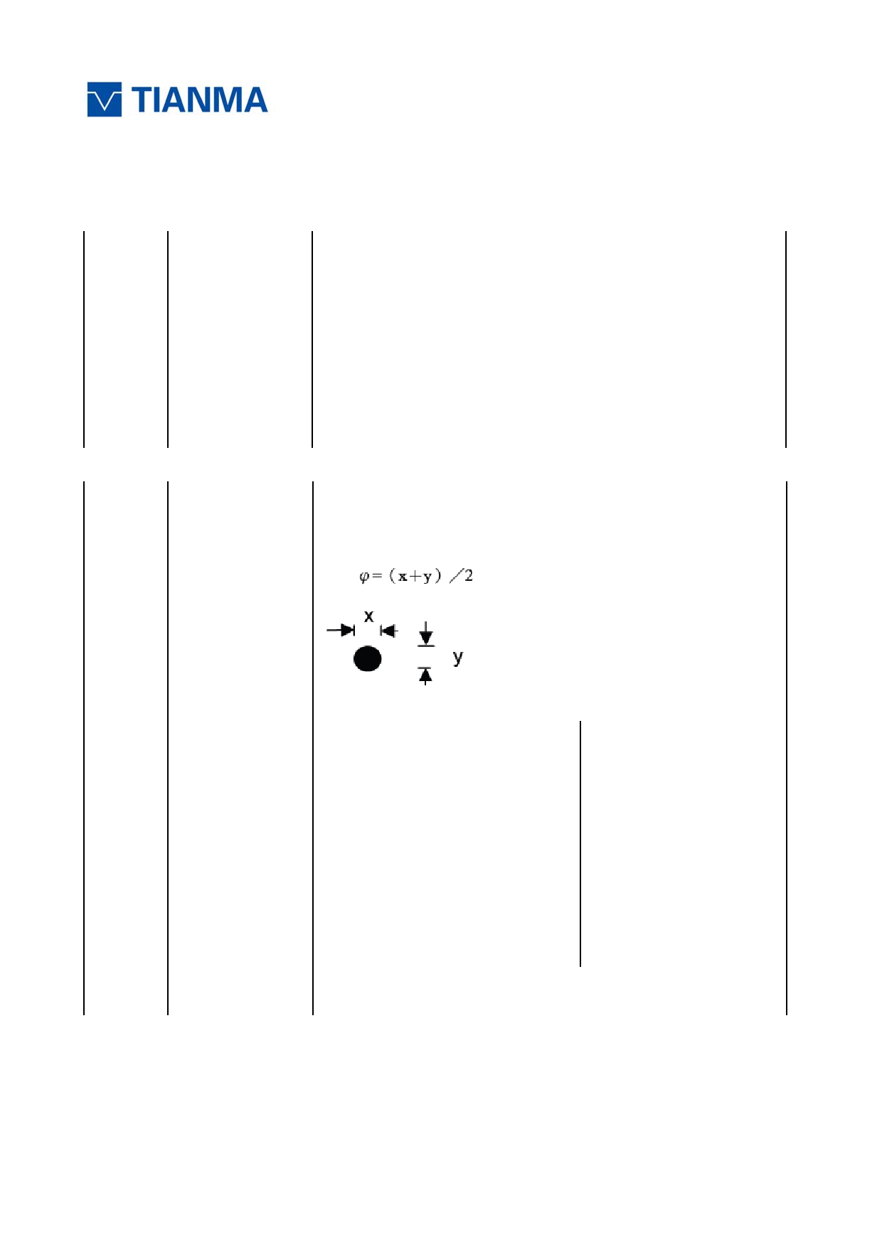
For dark/white spot is defined
Spot Defect
Including
Φ > 0.20 distance between spot must be larger than ≥ 5mm
Black spot
a
White spot
Size φ (mm)
Acceptable Quantity
Pinhole
Foreign particle
Polarizer dirt
φ≤ 0.20
Ignore
0.20 ﹤ φ≤ 0.50
3
0.50 ﹤ φ
Not allowed
b
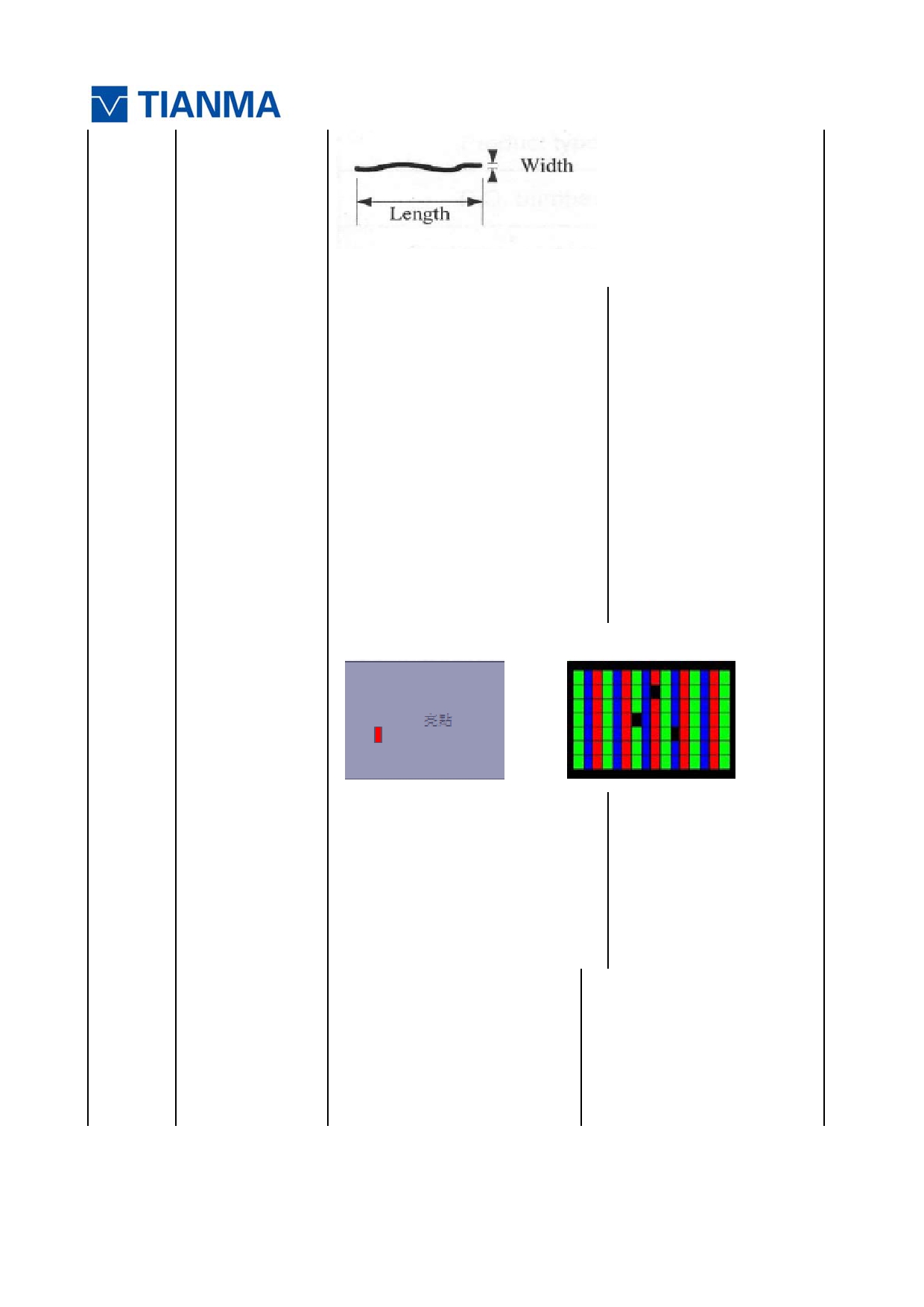
Line Defect
Define:
Including
The information contained herein is the exclusive property of TIANMA MICRO-ELECTRONICS Corporation
and shall not be distributed, reproduced, or disclosed in whole or in part without prior written permission of
TIANMA MICRO-ELECTRONICS Corporation.
Page 39 of 42
www.topwaydisplay.com
sales@topwaydisplay.com
+86(755)3699-5528
Shenzhen TOPWAY Technology Co., Ltd.
+86(755)8179-5700
Model No.TM101DDHG04
Black line
White line
Scratch
Distance between line defect ≥ 5mm
Width(mm) Length(mm)
Acceptable Quantity
W ≤ 0.05
Ignore
0.05 ﹤ W ≤ 0.1
L ≤ 2.0
4
0.1 ﹤ W
Follow a
Size φ (mm)
Acceptable Quantity
φ≤ 0.20
Ignore
c
Polarizer
Dent/Bubble
0.20 < Φ≤ 0.5
3
0.5 ﹤ φ
0
Bright and Black Sub Pixel define:
Sub Pixel
and
d
Electrical
Defect
Item
Acceptable Quantity
Black Sub Pixel defect
2
Bright Sub Pixel defect
0
Total Sub Pixel defect
2
Distance between black Sub Pixel
> 15mm
Broken
Not allowed
e
FPC
Crease
Can't resume is not allowed
Dirt
f
Bezel
Wrap
No harm
Broken
The information contained herein is the exclusive property of TIANMA MICRO-ELECTRONICS Corporation
and shall not be distributed, reproduced, or disclosed in whole or in part without prior written permission of
TIANMA MICRO-ELECTRONICS Corporation.
Page 40 of 42
www.topwaydisplay.com
sales@topwaydisplay.com
+86(755)3699-5528
Shenzhen TOPWAY Technology Co., Ltd.
+86(755)8179-5700
Model No.TM101DDHG04
Sunken
No dangerous
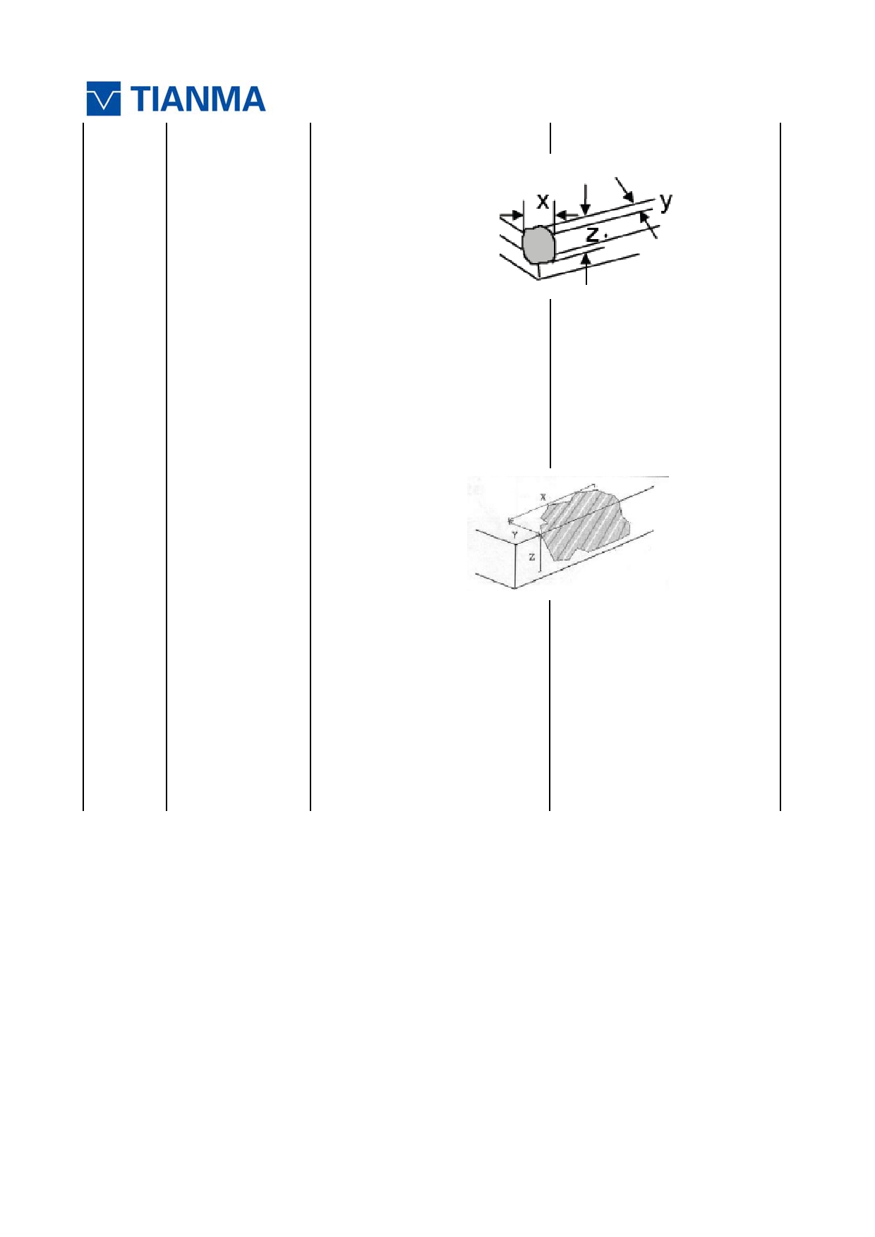
1.Corner Fragment:
Size(mm)
Acceptable Quantity
X ≤ 3mm
Ignore
Y ≤ 3mm
T : Glass thickness
Z ≤ T
X: Length
Y: Width
Z: thickness
g
Glass defect
2. Side Fragment:
Size(mm)
Acceptable Quantity
Ignore
X ≤ 6.0mm
T : Glass thickness
Y ≤ 1.0mm
X: Length Y: Width
Z ≤ T
Z: thickness
Note:
1. The AQL inspection sample method is applied for customer, not for SHTM. For SHTM does full
inspection in production line.
2. Dot defect is defined as the defective area of the dot area is larger than 50% of the dot area.
3. Mura is checker by 6% ND filter. ND application method: the parallel vertical distance between
ND and panel is 3~5cm , the distance of eyes look squarely to the panel is 30±5cm , checked by
3s.
4. Foreign particle on the surface of the LCM should be ignore.
5. The phenomenon that can be seen in all screen(Black 、 White 、 R 、 G 、 B),which seems like BL LED
light directly sending out through the panel ,need to be less than 1/3 dot.
The information contained herein is the exclusive property of TIANMA MICRO-ELECTRONICS Corporation
and shall not be distributed, reproduced, or disclosed in whole or in part without prior written permission of
TIANMA MICRO-ELECTRONICS Corporation.
Page 41 of 42
www.topwaydisplay.com
sales@topwaydisplay.com

+86(755)3699-5528
Shenzhen TOPWAY Technology Co., Ltd.
+86(755)8179-5700
Model No.TM101DDHG04
13.6. Mechanics specification :
As for the outside dimension, weight of the modules, please refer to product specification for more
details
13.7. Precaution
Please pay attention to the following items when you use the LCD Modules:
1. Do not twist or bend the module and prevent the unsuitable external force for display module
during assembly.
2. Adopt measures for good heat radiation. Be sure to use the module with in the specified
temperature.
3. Avoid dust or oil mist during assembly.
4. Following the correct power sequence while operating. Do not apply the invalid signal, otherwise,
it will cause improper shut down and damage the module.
5. Less EMI: it will be more safety and less noise.
6. Please operate module in suitable temperature. The response time & brightness will drift by
different temperature.
7. Avoid to display the fixed pattern (exclude the white pattern) in a long period, otherwise, it will
cause image stains.
8. Be sure to turn off the power when connection of disconnecting the circuit.
9. Polarizer scratches easily, please handle it carefully.
10. Display surface never likes dirt of stains.
11. A dew drop may lead to destruction. Please wipe off and moisture before using module.
12. Sudden temperature changes cause condensation, and it will cause polarizer damaged.
13. High temperature and humidity may degrade performance. Please do not expose the module to
the direct sunlight and so on.
14. Acetic acid or chlorine compounds are not friends with TFT display module.
Static electricity will damage the module; please do not touch the module without any grounded
device.
15. Do not disassemble and reassemble the module by self.
16. Be careful do not touch the rear side directly.
17. Not strong vibration or shock. It will cause module broken.
18. Storage the modules in suitable environment with regular packing.
19. Be careful or injury from a broken display module.
20. Please avoid the pressure adding to the surface (front or rear side) of modules, because it will
cause the display non-uniformity of other function issue.
The information contained herein is the exclusive property of TIANMA MICRO-ELECTRONICS Corporation
and shall not be distributed, reproduced, or disclosed in whole or in part without prior written permission of
TIANMA MICRO-ELECTRONICS Corporation.
Page 42 of 42
www.topwaydisplay.com
sales@topwaydisplay.com